@forr
Yes, some amps don't close the FB loop at the IPS or don't use FB at all. No error current. Your explanation is good in most cases and is appropriate for studying amp construction. I would probably tell the same if asked. My point is that there isn't strict universal definition to adhere to.
Joyeux Noël!
Last edited:
Transistors with a common base are voltage amplifiers.This is an axiom.
Common emitter transistor stages are also voltage amplifiers.
Transitors are transconductance devices, voltage controlled current sources.The common emitter is not only a voltage amplifier, but also a current amplifier.In contrast to a common base .
Per se, they are not voltage amplifiers which, by definition, are voltage controlled voltage sources.
To avoid (rare) confusions with VAS, second stage..., I often used "Main Voltage Amplification Stage".BTW, can we stop using the term 'VAS'? This is the ridiculuous term that Self coined. All non-audio literature uses the name 'second gain stage'.
Transitors are transconductance devices, voltage controlled current sources.
Being wired as common emitter/source.
The mode of operation of a transistor (common electrode) does not change its physical property of transconductance.Being wired as common emitter/source.
Transitors are transconductance devices, voltage controlled current sources.
That's just one way to model transistor, namely the popular h-parameters. There are other equally valid models like Admittance parameters (y-parameters), Inverse hybrid parameters (g-parameters), etc.
Two-port network - Wikipedia
The mode of operation of a transistor (common electrode) does not change its physical property of transconductance.
Now common collector and common emitter circuits becomes the same, thank you!
😀
Transconductance
Which is the model most used in the low frequency audio range, particularly by audio engineers who have written very often quoted books ?
Transconductance is an attribute of the elementary amplifying components which are : tubes, bipolar transistors and FETs.That's just one way to model transistor, namely the popular h-parameters. There are other equally valid models like Admittance parameters (y-parameters), Inverse hybrid parameters (g-parameters), etc.
Two-port network - Wikipedia
Which is the model most used in the low frequency audio range, particularly by audio engineers who have written very often quoted books ?
What is the mode of a transistor which has a degenerative resistor in series with its emitter and a resistor load at its collector ?Now common collector and common emitter circuits becomes the same, thank you!
It used to be called "split loads" on similar valve circuits.
The voltage follower property of the emitter is not lost. The emitter voltage stays almost the same as in a pure common mode collector (= emitter follower). This property is very rarely quoted in litterature.
Roughly, the transistor gm calculated from collector current Ic gives the output resistance of the emitter (~ 1/gm) and the voltage across the collector load.
Dividing the value of the collector resistor by the sum of the emitter resistance and the degenerative resistor gives a good approximation of the circuit voltage gain.
Using transconductance is more clear and efficient than trying to think in mode terms where the above circuit should be described as working in a double mode.
Last edited:
The input stage of a feedback amplifier has a non-inverting input and an inverting input. It converts the voltage difference between these two inputs to a current which is sometimes wisely called the error current.
The input stage stops at the point where this current is delivered. This is here that the next stage begins. The error current can be exploited using different ways,
Could an input stage work differently ?
The node where the input stage current gets delivered and hence the node where the next stage starts (be a second gain stage or the output stage in single gain stage amps) is the first high impedance node or HiZ1.
Let's split hair little bit, purely academic. It's still valid to say VT5 is voltage amplifier. Current from GM cell is converted to voltage by the (low) input impedance of VT5 (emitter). This small voltage is then amplified by VT5.
This is true, bur does not make VT5 part of the second gain stage. As in my prev. post, the second gain stage starts after the first HiZ node (collector of VT5). The emitter of VT5 is low impedance.
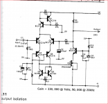
The main thing is that such a cascode allows you to get a very large loop gain of 92dB at 20kHz and very low distortion.
Last edited:

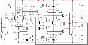
It is usually called a Rush circuit, consisting of two complementary transistors having coupled emitters. It acts as a differential circuit. The first time I saw it was on the circuit of Ed Cherry's NDFL amplifier.Something a bit different.

Considering a Rush circuit as a cascode is a common error.
Another Cascode Example
The 2k7 load resistor would normally be replaced by a constant current source. The value of 2k7 possibly with 2000 pF in parallel was thought to be representative of the gain stage load presented by an output stage.
The author published a design in 1972 than had a buffer ahead of the gm transistor. The buffer was dc bootstrapped with phase correction strung networks around this.
This was one of a series of amplifiers I have built. It needed a better pre-amp I than the IC based one I had at the time.
I am responding to the initial request - take it or leave it.
Attachments
Mjona,
I probably don’t get the point.
Are you trying to tell with this simple and straightforward two stage SE amp, that cascoding helps to give you a high gain ?
Hans
I probably don’t get the point.
Are you trying to tell with this simple and straightforward two stage SE amp, that cascoding helps to give you a high gain ?
Hans
Mjona,
I probably don’t get the point.
Are you trying to tell with this simple and straightforward two stage SE amp, that cascoding helps to give you a high gain ?
Hans
The calculated gain for this 1990 circuit I posted was 330,000 at 1kHz. There were no computer simulations. If you can find circuits that gives this much at 1Hz you can judge for yourself.
- Home
- Amplifiers
- Solid State
- Comparative VAS+cascode stage