post34 tells you.Sort things out is exactly what I'm trying to do. But if you won't point out where on the posted schematic you see an error, then how do you think that could be possible?
I'm simply asking that you indicate where on the posted schematic any error might be. Everything is labeled, so simply indicate, that's all I'm asking.
.
post38 expands on that.
... At bottom I'm trying to come up with something that will answer the newbie's inevitable question, "How am I supposed to connect all these ground thingees together?" Come up with something simple enough to be usable...
I guess I belong to one of those newbie, was trying to build my first power amplifier couple of months ago, and here is my personal experience:
- When everything was ready and I needed to put them together in a chassis, like many newbie I searched in this forum on how to ground properly ...
- I found some posts by OP, advocating the scheme you're proposing in this thread. I found some posts by many others, recommending something very different ... as a newbie I was entirely confused.
- As the star ground concept seemed sexy, I tried using it - and there was a problem, it leaves many sections of wiring which are alone and cannot be twisted. I didn't feel comfortable with it so I switched to the other camp.
- I used the "minimizing the loop area" method then, wiring are mostly twisted and I felt more comfortable. The amp is dead quiet using this scheme.
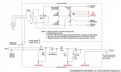
In your scheme at post #67, for example, for the audio output, how can one twist the audio return line all the way to point B? The best I could do was to twist the wire with the audio signal back to the audio circuit PCB, and then the audio return line has to go to point B alone, untwisted.
Please forgive me if this is a stupid question from a newbie.
Last edited:
In your scheme at post #67, for example, for the audio output, how can one twist the audio return line all the way to point B? The best I could do was to twist the wire with the audio signal back to the audio circuit PCB, and then the audio return line has to go to point B alone, untwisted.
You came to the same conclusion as I did, one solution is to move point B to the output. This is also a good place to start your layout design.
The speaker current flows from the PSU through the amplifier.
The speaker return current has to follow the same route back to it's source.
The speaker return current has to follow the same route back to it's source.
So we could place local GND (B) near to the output of the opamp, run a clean GND and +/- rails from the PSU to the opamp. Or even better as suggested by Bonsai in post 45: +/GND GND/- from two PSU to the opamp.
This is also starting to look a lot like the advice given by TI in their LM datasheets.
This is also starting to look a lot like the advice given by TI in their LM datasheets.
Which post shows the sch you are referring to?So we could place local GND (B) near to the output of the opamp, run a clean GND and +/- rails from the PSU to the opamp. Or even better as suggested by Bonsai in post 45: +/GND GND/- from two PSU to the opamp.
This is also starting to look a lot like the advice given by TI in their LM datasheets.
No schematic yet, just thinking out loud, trying to translate the rules into a layout, working backwards from output to chip to PSU.
The closest so far would be the one at post#2
The closest so far would be the one at post#2
.
Thanks for your post, cwtim01. I'm extremely interested in your experience and I'm giving it study. "Giving it study" means I have no immediate answers to your questions so I'm trying to figure some out. This is exactly what I was hoping for in the first place, so thanks.
While that goes on I think I'll mention one or two things. Maybe three.
<< Please forgive me if this is a stupid question from a newbie. >>
You kidding? Yours is the most intelligent post in this thread. By no means excluding mine.
<< I do believe "A wire placed in a varying magnetic field will have a varying current imposed along it...." >>
I'm guessing you misspoke, you meant "understand," not "believe." The quoted writer speaks of the principle of magnetic induction, which may have been known to the ancient Greeks (500 BC), but in any case was codified in the early 1830s. It's how transformers, speakers, and electric motors work, among many other devices.
Changing the subject entirely, speaking now of present cases, the "twisted pair" concept is handed down to us from telephone wiring practice. It's been used since around 1881.
Printed circuit boards obviously can't have twisted pairs, so to "minimize loop area" is, broadly speaking, the flat-world application of the twisted pair concept. For this reason the term is more often applied to printed circuit boards than to point-to-point wiring, although the principle is of course valid for all conductors.
All this is known science, commonly taught in basic electronics courses. Then one might wonder: what's all the ruckus?
You might notice that I keep asking people to indicate where on the posted schematic they see a problem with loop area, or with twisted pairs.
Of course that can't be done because schematics don't show loop area, or twisted pairs. Those are real-world wiring, which is dealt with in printed circuit board layouts, or in circuit notes. Nothing to do with schematics at all.
So the ruckus is people avoiding saying "it's nothing to do with the schematic, it's just an idea I had." Which might be very good ideas, but they're ideas that have nothing to do with the business at hand.
Neither do "ground lift" schemes of various names. In my opinion all such schemes are: a) Sloppy workarounds. b) Dangerous. c) Quite possibly illegal. But whatever else they may or may not be, they're not something that relates to the business at hand.
There is, in fact, business at hand. My job now is to reconcile theory with real-world reports of problems, and posted questions. I wonder if I'll be able to do this? The excitement builds.
.
Last edited:
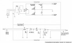
post2 has no "B" shown.So we could place local GND (B) near to the output of the opamp, run a clean GND and +/- rails from the PSU to the opamp. Or even better as suggested by Bonsai in post 45: +/GND GND/- from two PSU to the opamp.
This is also starting to look a lot like the advice given by TI in their LM datasheets.
What is of concern is that people are trying to build these Bentsnake schematics. They are posted as the best layout possible.
Indeed the excitement builds.
Indeed the excitement builds.
That is precisely the problem
Bentsnake has posted dozens of these incorrect and/or misleading schematics in various Threads, many intended for Beginners who know no better than Bentsnake.
Bentsnake has continued to post these erroneous schematics after being informed that they are misleading !
Part of the "problem" is that Bentsnake cannot see that labeling everything as GND is the single most confusing item on this Forum.
Bentsnake schematics
Not mine. What, I'm making this stuff up? Not.
.
how to create good drawings quickly.
Create a schematic in LTspice or similar. Take a screenshot.
(Take a screenshot by hitting the Printscreen key. Nothing visible happens, but what you see on the monitor is now on the clipboard.)
Paste the screenshot into paint.NET. Edit as wished.
After you have a few schematics in a folder you can pretty much copy-paste between them, new schematics are not needed all that often.
Note 1: You want all the components the same size, of course. Using LTspice's viewing option of Zoom to Fit (right click) usually does this, but other times you have to fiddle.
Note 2: If you don't know, the LTspice background color can be changed in Tools ~> Control Panel ~> Drafting Options ~> Color Scheme. You can also get rid of those annoying dots, which LTspice calls grid points.
Most Important Note: The grid point dots might annoy me personally, but this is in no way intended as finding fault with LTspice. Many thanks to Linear Technology for making this great program available.
.
Last edited:
Or come to think of it, you could just paste the screenshot into IrfanView or similar, save it as a .jpg, and upload it unedited.
You can do a limited amount of editing in IrfanView. For instance select just the schematic part of the screenshot and save that.
You can do a limited amount of editing in IrfanView. For instance select just the schematic part of the screenshot and save that.
Last edited:
.
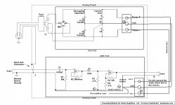
Meanwhile, it might be helpful to post a slightly updated version. Not actually for itself, but for the purely schematic version, which is also posted.
The two circuits are electrically the same, so maybe having them side by side will be convenient for comparison.
.
Meanwhile, it might be helpful to post a slightly updated version. Not actually for itself, but for the purely schematic version, which is also posted.
The two circuits are electrically the same, so maybe having them side by side will be convenient for comparison.
.
Attachments
We are not making any progress. You Post your schematic, it is explained what is wrong and how to fix it, you disregard both and start all over again.
Why don't you try it out and make some measurements?
It does not make mutch sense to talk about grounding without some concrete problem at hand.
Anyway i bet that most amp designs are noisier than a simple star ground...
A way how to measure ground introduced noise is the Hummer Test (see fig 1):
AV: How To Find Problems That Degrade Performance In Balanced Audio Equipment Interfaces - Pro Sound Web
Bill Whitlock has also a wealth of info:
An Easily Implemented Procedure for Identifying Potential Electromagnetic Compatibility Problems in New Equipment and Existing Systems:
- Status
- Not open for further replies.
- Home
- Source & Line
- Analog Line Level
- Comment on Grounding Scheme?