.
If separate amp and PSU boards are used, then point B would probably be on the amp board, not on the PSU board. So I'm thinking doors66 has a logical approach.
Also thinking that conductor A-B is an audio line, so possibly a shielded conductor. Except I have no idea how to connect the shield.
<< Why don't you try it out and make some measurements? >>
The theory's being reexamined so there's nothing to build yet.
.
Those new block showing power/gnd/-power are basically connectors on the pcb. So point B is the gnd connection point on the power connector (or a solder pad) on the psu pcb. The other connector showing vcc/gnd/-vcc is on the amp pcb. So A-B is a trace on power pcb..
If separate amp and PSU boards are used, then point B would probably be on the amp board, not on the PSU board. So I'm thinking doors66 has a logical approach.
Also thinking that conductor A-B is an audio line, so possibly a shielded conductor. Except I have no idea how to connect the shield.
<< Why don't you try it out and make some measurements? >>
The theory's being reexamined so there's nothing to build yet.
.
Those new block showing power/gnd/-power are basically connectors on the pcb. So point B is the gnd connection point on the power connector (or a solder pad) on the psu pcb. The other connector showing vcc/gnd/-vcc is on the amp pcb. So A-B is a trace on power pcb.
Yes, I see that you've moved connectors from one board to the other. Logical way to go.
However, I wonder about twisting the triplet Vcc/gnd/Vee. I don't mean I disagree with it, I just wonder about it. Even after filtering the Vee/Vcc lines are not perfect DC, so...well, so I wonder.
The pic below is actually basically the same as yours, just laid out horizontally. Sometimes moving the blocks around makes something show up.
The more I think about my shielded conductor idea, the less I like it.
<< Why don't you try it out and make some measurements? >>
Actually, I think I will lay out some parts, see what things look like.
.
Attachments
Last edited:
Two steps forward, one step back. Your schematic is not "basically the same".
You have again split the audio GND into two parts instead of an Audio GND with a single connection to Power GND and you have moved the Bypass GND back to A.
I still think that if you actually placed the Bypass Capacitors in your schematic things would be more obvious to you why your layout is so wrong.
In the category " So the why is 'cause he says so".
"The contribution of Distortion 6 can be reduced below the noise floor. Firstly, rigorously minimise loop areas in the input and feedback circuitry, ie keep each signal line very close to its ground. Secondly, limit the ability of the supply wiring to establish magnetic fields in the first place, by minimising the area of circuit loops carrying half- wave pulses." - D. Self.
This clearly describes how the Audio GND and the supply rails should be designed according to D. Self.
Last edited:
I have added the caps.
Wait a sec. I thought before that I understood what you were doing in post 99, but now I don't think I did.
It seems you're picking up the whole shebang from the PSU board, and moving it to the amplifier board? Hmmm.
.
Either you merge them on the amp board itself, or you run a separate line back to the psu board. Or do you merge C, D and F into one point by using a ground plane. Thats what we are discussing, whats the best way to do this. The image probably shows a common way to do it where there is a single ground return connection between amp pcb and psu pcb, rather than dedicated ones for different returns.Wait a sec. I thought before that I understood what you were doing in post 99, but now I don't think I did.
It seems you're picking up the whole shebang from the PSU board, and moving it to the amplifier board? Hmmm.
.
Last edited:
Wait a sec. I thought before that I understood what you were doing in post 99, but now I don't think I did.
It seems you're picking up the whole shebang from the PSU board, and moving it to the amplifier board? Hmmm.
.
Take a look at some amp and preamp boards, see how many of them allow you to return a audio return, decoupling return etc back to the psu pcb. Most of them I have seen merge all these on the amp pcb itself and return a single ground line back.

I guess I belong to one of those newbie, was trying to build my first power amplifier couple of months ago, and here is my personal experience:
To be honest I didn't listen with your grounding method, so not sure if it is also quiet or may hum, but I do believe "A wire placed in a varying magnetic field will have a varying current imposed along it...." so maybe you could help me with this (for my next amplifier):
- When everything was ready and I needed to put them together in a chassis, like many newbie I searched in this forum on how to ground properly ...
- I found some posts by OP, advocating the scheme you're proposing in this thread. I found some posts by many others, recommending something very different ... as a newbie I was entirely confused.
- As the star ground concept seemed sexy, I tried using it - and there was a problem, it leaves many sections of wiring which are alone and cannot be twisted. I didn't feel comfortable with it so I switched to the other camp.
- I used the "minimizing the loop area" method then, wiring are mostly twisted and I felt more comfortable. The amp is dead quiet using this scheme.
In your scheme at post #67, for example, for the audio output, how can one twist the audio return line all the way to point B? The best I could do was to twist the wire with the audio signal back to the audio circuit PCB, and then the audio return line has to go to point B alone, untwisted.
As I said before, all good questions. Certainly good enough to throw me for a loop...no pun intended. But after some thought and re-study I think I can provide answers.
As usual, the answers are one step earlier. That is, what appears to be a problem now isn't one at all. The real problem is one that occurred earlier and was left unsolved, so now, later, it's multiplying and screwing the works.
The earlier unsolved problem in this case is the sister concepts of "twisted pair" and "minimize loop area." I say sister concepts because they're both actually the same concept, which is, broadly, "minimize inductive effects." But "twisted pairs" applies to point-to-point wiring, while "minimize loop area" usually applies to printed circuit boards, which obviously can't have twisted pairs.
I think the exact problem is not understanding what a "pair" is, so herewith a definition. A pair is two conductors that feed-from, and return-to, the same source. The "source" might be many things, a transformer, a battery, an op amp, a wall receptacle, but in all cases a "pair" feeds from and returns to that same source.
Other conductors are not pairs, and are not to be twisted together with each other. Emphasizing that, do not just twist random wires together because it looks neat.. There's no evidence that electrons care about neat.
It's really as simple as that. Pairs is pairs, others ain't. So getting to specific questions:
<< the star ground concept...I tried using it - and there was a problem, it leaves many sections of wiring which are alone and cannot be twisted >>
Right, and as above they're not supposed to be. Just as every trace on a printed circuit board is not "paired" with some other trace.
<< In your scheme at post #67, for example, for the audio output, how can one twist the audio return line all the way to point B? The best I could do was to twist the wire with the audio signal back to the audio circuit PCB, and then the audio return line has to go to point B alone, untwisted. >>
Right again, and again, that's the way it's supposed to be. Obviously a pair must separate at some point, since the two conductors don't connect to the same terminal. So the answer is you do it and don't worry about it, it's not going to hurt anything. The idea is to minimize inductive effects, not to eliminate them (which is impossible). Also see below about easy.
<< To be honest I didn't listen with your grounding method, so not sure if it is also quiet or may hum...I used the 'minimizing the loop area' method...The amp is dead quiet using this scheme. >>
Right yet again--although do bear in mind that "minimize loop area" and "twisted pairs" are the same concept applied to two different situations (printed circuits vs. point-to-point). No doubt you took care to keep your audio conductors away from the power supply conductors, and that's 99% of the battle right there (the other 1% is taking care with your solder joints--I recommend always using flux).
Now speaking more broadly, please don't think I'm trying to take anything away from cwtim01 (I'm not) when I proclaim again and yet again: chip amps are supposed to be easy in the first place, and they will be if you don't make them complicated. They're easy because the engineers already did the heavy lifting for us.
The upshot is that success is assured as long as we follow a few basic rules of thumb. Except...sometimes those rules of thumb are not as clear as we might wish. Especially in the case of how to run return and ground (they are NOT the same thing) conductors.
Hence this thread: my effort to codify and simplify. Only to discover that what I thought was crystal clarity turned out to be all murk and confusion to cwtim01. Valuable information, that, and thanks again to cwtim01 for posting his questions. In a day or so I'll try again.
.
Last edited:
So far you have this right.................. A pair is two conductors that feed-from, and return-to, the same source. The "source" might be many things, a transformer, a battery, an op amp, a wall receptacle, but in all cases a "pair" feeds from and returns to that same source.
Every "circuit" must form a loop. That loop brings the current from the source AND returns the same current to the source.
WRONG !!!!!Other conductors are not pairs, and are not to be twisted together with each other. Emphasizing that, do not just twist random wires together because it looks neat.. There's no evidence that electrons care about neat.
It's really as simple as that. Pairs is pairs, others ain't. So getting to specific questions:
<< the star ground concept...I tried using it - and there was a problem, it leaves many sections of wiring which are alone and cannot be twisted >>
Right, and as above they're not supposed to be. Just as every trace on a printed circuit board is not "paired" with some other trace.
<< In your scheme at post #67, for example, for the audio output, how can one twist the audio return line all the way to point B? The best I could do was to twist the wire with the audio signal back to the audio circuit PCB, and then the audio return line has to go to point B alone, untwisted. >>
Right again, and again, that's the way it's supposed to be. Obviously a pair must separate at some point, since the two conductors don't connect to the same terminal. So the answer is you do it and don't worry about it, it's not going to hurt anything. The idea is to minimize inductive effects, not to eliminate them (which is impossible). Also see below about easy.
a source sends out current. That current MUST return to the source from whence it came. There are no exceptions.
All that follows seems just as mixed up. Sources send current around a circuit.
To minimise the interference effects minimise the Loop Areas. That includes traces on a PCB and includes point to point wiring and includes wiring between the terminals of big two lead passives, eg. capacitors and rectifiers.
the confusuion was not to Cwtim. It was your complete misunderstanding of and continues to be your non acceptance that current flows from the Source and MUST RETURN to the Source for every "circuit".<< To be honest I didn't listen with your grounding method, so not sure if it is also quiet or may hum...I used the 'minimizing the loop area' method...The amp is dead quiet using this scheme. >>
Right yet again--although do bear in mind that "minimize loop area" and "twisted pairs" are the same concept applied to two different situations (printed circuits vs. point-to-point). No doubt you took care to keep your audio conductors away from the power supply conductors, and that's 99% of the battle right there (the other 1% is taking care with your solder joints--I recommend always using flux).
Now speaking more broadly, please don't think I'm trying to take anything away from cwtim01 (I'm not) when I proclaim again and yet again: chip amps are supposed to be easy in the first place, and they will be if you don't make them complicated. They're easy because the engineers already did the heavy lifting for us.
The upshot is that success is assured as long as we follow a few basic rules of thumb. Except...sometimes those rules of thumb are not as clear as we might wish. Especially in the case of how to run return and ground (they are NOT the same thing) conductors.
Hence this thread: my effort to codify and simplify. Only to discover that what I thought was crystal clarity turned out to be all murk and confusion to cwtim01. Valuable information, that, and thanks again to cwtim01 for posting his questions. In a day or so I'll try again.
.
Last edited:
WRONG !!!!!
No, right, actually.
For the benefit of casual passers-by, maybe I should point out that AndrewT appears to be speaking of basic theory, while I'm talking about real-world application. The subject at hand is not how current flows, the subject is how to connect the wires so it can flow.
.
.
Just to mention it, if everybody in the world is going to repost images I made, then they might at least give me a word of credit. Maybe even a link to bentsnake.com.
"Huh? Wait a minute bubba! You're mostly posting Douglas Self's circuits, you don't get credit for that!"
Yes that's true, if you believe that Mr. Self's circuits jumped out of his book, transformed themselves into .jpg images, and posted themselves to the Internet.
Otherwise, yes the circuits are his, but the images are mine. Which is to say we share ownership. Don't worry, I'm going to send Mr. Self his cut of the millions I know I'm going to make.
But until that particular cash cow starts mooing you'll notice I take care to credit Mr. Self's work to him. In some circles it's considered the right thing to do.
.
For the benefit of casual passers-by, maybe I should point out that AndrewT appears to be speaking of basic theory, while I'm talking about real-world application. The subject at hand is not how current flows, the subject is how to connect the wires so it can flow.
.
 ... AndrewT knows what the hell he is talking about. If you want to solve your problem you should ramble less and show forum members like him your real world diagrams or pictures of whatever project you are no doubt butchering.
... Certainly good enough to throw me for a loop...no pun intended. But after some thought and re-study I think I can provide answers ...
Thanks for taking the time and effort to answer my question, not sure if I agree but I didn't expect such simple question would require so much thinking from a guru, as I thought you must have encountered it before in actual amplifier builds.
Would be nice if you could share some details of your real-world applications of your proposed grounding method.
Last edited:
Thanks for taking the time and effort to answer my question, not sure if I agree but I didn't expect such simple question would require so much thinking from a guru, as I thought you must have encountered it before in actual amplifier builds.
Would be nice if you could share some details of your real-world applications of your proposed grounding method.
Hey what? Me, a guru? Hang one, I have to check with my gf.
She says no. On the present subject, you ask about real-world applications. You want to see see photographs? A reasonable and productive request, but sorry I have none. Good idea, though. In fact, excellent idea.
What I do have right now is as before: the intention that newbies will be able to solder up a simple chip amp without it becoming a life changing event for them. Or without being told to enroll in an electronics course, or to go out and buy a $2,000 oscilloscope, as is known to happen around here.
To that end yet another revision is in the works. Day or so.
.
Hey what? Me, a guru? Hang one, I have to check with my gf.
She says no.
WTF? This is the kind of weird stuff you can go ahead and leave out of your posts, you will get better advice from people if you do.
the intention that newbies will be able to solder up a simple chip amp without it becoming a life changing event for them. Or without being told to enroll in an electronics course, or to go out and buy a $2,000 oscilloscope, as is known to happen around here.
I think you've been given some good advice about some fundamentals that will help your project be better if you think about them while you lay out your chip amp.
I get it, chip amps are more simple than discrete but it's not like an A/V receiver where you just hook cords up and go. The stuff you hook up to a chip amp matters and how you wire those things in matter.
That's why showing your design in pictures or diagrams/schematics helps you get the solution so much faster.
.
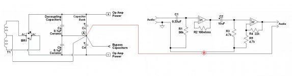
The goal is to illustrate a practical grounding scheme, while keeping the audio signal separate from all other voltages and currents.
Isolating the audio signal is desirable because all conductors have at least some resistance, however small. The result is that the conductors in an audio circuit form, in effect, a mixing board. This can mix power supply and other signals directly into the audio signal, causing noise and distortion.
These problems are usually (not always) very small, but they can add up. So the idea is to avoid problems in the first place by keeping the audio signal isolated.
Corrections/comments/questions are much wanted, especially if you're new to this stuff and think you're asking a dumb question, which you're not.
CIRCUIT NOTES:
A is circuit ground. As always there is one circuit ground point, and one only.
B is audio common, also called star ground, or star point. All audio returns (in red) are routed to this single point. As with circuit ground there is one audio common point, and one only.
NOTE: Points A and B may be very close together (perhaps 1/8"), but they must be separate terminals.
C is a bus line for the bypass capacitors (if used). This might be the most practical way to return these capacitors to circuit ground.
D is the chassis bond, which is its correct name. Usually this is called chassis ground or safety ground, but speaking correctly there's no such thing as either. It's a "bond," as in "bonded to earth." Here I'm using the correct name to, again, keep circuit ground (point A) as the single ground point.
NOTE: there is one chassis bond point and one only, located near the audio signal input as shown. But if there are two metal housings, as for a remote power supply, then of course there's one (only) bonding point for each.
WIRING NOTES:
"Twisted pairs" are feed-and-return pairs only, do not twist in additional conductors.
Only two exceptions come to mind: twisting the three conductors connecting to a potentiometer, or the three secondary conductors of a center-tapped transformer. In any case NEVER twist audio signal conductors together with power supply conductors.
It's understood that it's not always feasible to lay out an ideal circuit. But in every case try not to mix the return of the audio input signal with any other until point B (audio common) is reached. The input is the single most delicate signal in any circuit, so protect it in any way you can.
The shown circuit should be considered as a practical method, but not as "the only right way to do it." Generally, remember to apply the principle of "separate the audio signal from all other voltages and currents" and your circuit will be fine.
.
Attachments

.
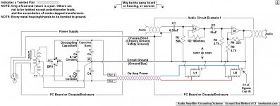
...while for clarity, I hope, and contrast, posted below is the all into one grounding method. As a matter of fact this method has worked fine in many circuits, but when it comes to avoiding noise and distortion there is a certain element of luck involved. That's the purpose of the star ground method posted above, not depending on luck.
.
Attachments
- Status
- Not open for further replies.
- Home
- Source & Line
- Analog Line Level
- Comment on Grounding Scheme?