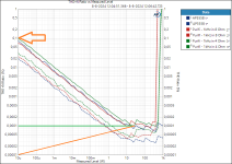
You misunderstand. What you point to is close to the residual of the 555B. So it is impossible to say what the class D contributes, other than it is similar to the AP.That graph shows me typical class D amps imperfection ,I consider such class D amp that have 0,1% THD&N characteristic (which is nothing special IMHO) , regardless that in range between 1W and up to full power THD&N is much lower , also I will be interested to see what is the real level of output RF noise spectrum at full output power near to clipping or even at clipping point .
Jan
I tested the DoubleCross circuit in my simulator. I made the following observations:
* Using two pairs of output transistors reduces distortion because each transistor handles only half of the load current. For fair comparison, the baseline class AB circuit should also have two pairs of output transistors.
* Reducing the value of the emitter resistors reduces distortion, especially in case of overbias. The downside of smaller resistors is that the amplifier has less margin against thermal runaway.
When I apply both techniques to the class AB amplifier, I see similar THD as the DoubleCross amplifier.
Ed
yes I did noticed that , but again at 1mW measured THD&N is 0,01% (still nothing special), anyway IMHO it will be much better amp if THD vs output power characteristic is flat (green line) , or is inverse to actual measured data (orange line) ,Did you notice that 0.1% THD+N is for 10 uW output level?
Essentially, it’s just noise at extremely low level. Not even Benchmark AHB2 or Topping B200/B100 are close.
btw , do you have any information what is the output level of generated RF signals at full output power ?
Attachments
Green line is impossible for THD+N as noise becomes larger part of combined THD+N at low levels, but it could be possible for THD alone.IMHO it will be much better amp if THD vs output power characteristic is flat (green line)
Of course not.btw , do you have any information what is the output level of generated RF signals at full output power ?
Hopefully, that will be provided by Jan, or maybe someone at ASR forum.
RF is my concern as well.
Again, you don't understand. At 1mW it is only noise, no distorrtion.yes I did noticed that , but again at 1mW measured THD&N is 0,01% (still nothing special), anyway IMHO it will be much better amp if THD vs output power characteristic is flat (green line) , or is inverse to actual measured data (orange line) ,
btw , do you have any information what is the output level of generated RF signals at full output power ?
Jan
Yes noise dominates at low levels because the THD is lower than the noise.Green line is impossible for THD+N as noise becomes larger part of combined THD+N at low levels, but it could be possible for THD alone.
I don't understand your statement above. Clearly, the green line is possible - it's there.
Jan
I’m referring to horizontal green THD+N line, manually added to chart by banat at post #43.I don't understand your statement above. Clearly, the green line is possible - it's there.
OK, I see. If it would be THD-only it could make sense, and I think he meant it that way.
Or the orange line.
It becomes a measurement problem and an FFT would make that possible.
Jan
Or the orange line.
It becomes a measurement problem and an FFT would make that possible.
Jan
OK, I will soon add German subtitles to my videos. Sorry, I do not know German ...
Many thanks Nick,
it would be great if we could communicate extensively in each other's native language - unfortunately we have no choice but to take the detour across the English bridge.
Even though I'm not a linguistic whiz myself, English is enough for me personally. You are honored that you want to try a direct transfer into German.
Basically, I find your commitment to writing generally understandable explanations (using MC12, as a video tutorial) exemplary.
I'm probably just not the right addressee, because of course I already know in advance what you're about to click on - and want to show.
But that should not be my concern or even the topic of discussion here - as the chosen medium of expression, it is a path that you are consistently pursuing, and you are doing it very well, my sincere compliments.
#
For free, open and further discussion, it would be helpful if you put the circuit diagram here, I can read and understand it - to protect your idea, you could leave out some component values.
As I said, if I could speak your language, I would be happy to ask you specific questions - nothing is more enriching than an open exchange of ideas at eye level.
Now back to the topic "doublecross Class AB-BA"
All the best,
HBt.
"Offene Türen einrennen"
I know the short Leach essay - and I agree with you wholeheartedly.
Personally, I see the use of the term gm-doubling (as a synonym for a certain technical issue) as problematic, because it is (can be) misleading - and in my view is unsuitable for correctly visualizing what is going on (as a model). If you understand the model-view, you also understand the synonym.
However, this digression should not be the subject of discussion here. Just so much, I'm glad to see that I'm not technically alone - but i understand the term gm-doubling (and what it is supposed to convey in context).
greetings,
HBt.
Psst
back to ABBA doublecross
Hello Alex,there is no such thing as Gm doubling. There is a nice, if a bit math-heavy, note on this topic by Marshall Leach (attached). (...)
I know the short Leach essay - and I agree with you wholeheartedly.
Personally, I see the use of the term gm-doubling (as a synonym for a certain technical issue) as problematic, because it is (can be) misleading - and in my view is unsuitable for correctly visualizing what is going on (as a model). If you understand the model-view, you also understand the synonym.
However, this digression should not be the subject of discussion here. Just so much, I'm glad to see that I'm not technically alone - but i understand the term gm-doubling (and what it is supposed to convey in context).
greetings,
HBt.
Psst
back to ABBA doublecross
Here are some graphs from my simulator. These show the open-loop THD versus total bias current for a range of signal amplitudes (in peak volts).
Both amplifiers have two pairs of output transistors, 0.22ohm emitter resistors, and 4 ohm loads.
The Class AB amplifier has an optimum bias current of 200mA. We'll assume that the bias may drift up to 400mA with good thermal control. The rated THD would be 0.12% divided by the loop gain.
The DoubleCross amplifier has 150mV offset between the two pairs of transistors. The optimum bias current is 300mA which we'll assume may drift up to 600mA with good thermal control. The rated THD would be 0.08% divided by the loop gain.
It is cool to see the additional cancellation points in the DoubleCross amplifier. So, thanks for that!
The DoubleCross amplifier has less margin against runaway since the bias current is higher and largely flows through one pair of transistors.
The graphs illustrate the difficulty in relying on cancellation. I think that a 2:1 variation in bias current with temperature is quite good for discrete transistors.
Ed
Class ACDB
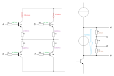
Does this sketch reflect the (simple) secret: I_R1 = I_R2 / 1.25 and vice versa I_R2 = 1.25 * I_R1 ..?

greetings,
HBt.
Does this sketch reflect the (simple) secret: I_R1 = I_R2 / 1.25 and vice versa I_R2 = 1.25 * I_R1 ..?
greetings,
HBt.
Compared to equal emitter resistors, using 25% larger resistors in the pair with lower bias results in less distortion at low amplitudes and more distortion at high amplitudes.
Ed
Ed
Ok, I get / understand it.Compared to equal emitter resistors, using 25% larger resistors in the pair with lower bias results in less distortion at low amplitudes and more distortion at high amplitudes.
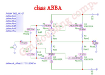
If I interpret Nick correctly, then Q1 and Q2 are not necessarily identical types in his circuit (nor are Q3 and Q4) ... without really thinking (please forgive me for this), I intuitively wrote a few values from Nick's comparison of the three published variants on the sketch! What value would R10 have to assume in order for the assumed ratio of the currents to be possible and in which decisive parameters would Q1 and Q2 have to differ?
I apologize in advance for any possible goofs in my own brainstorming.
#
Somehow I still can't really grasp Nick's AB-BA, while in contrast Yamaha's M2 immediately makes sense to me.
kind regards,
HBt.
Attachments
AFAIK Nick uses 0.25 ohm with the pair biased at ~100mA and 0.15 ohm with the other one, biased at ~35 mA. All transistors are 0281/0302, but the first pair are ThermalTraks (NJLxxxx), while the other is not (NJWxxxx).
+1. Two pairs biased at 70mA each should be more linear.I still can't really grasp Nick's AB-BA
Attached 'alexcp' sim, but manually optimised for 0.22 Ohm and 0.18 Ohm emitter resistors - see the purple wingspread plot at 160mA and 21mA idle currents below (green is a standard dual stage):

The wider linear Class-A region extends to about 4 watts peak. The dual standard bias can be optimised for a flat low distortion region, but it extends to only 160mW for similar value emitter resistors. Clearly the Double Cross method has extended Class-A region of low distortion before global feedback.
But this linear region is tricky to bias and depends to some extent on optimised values for the two sets of emitter resistors. Also it assumes the optimum bias conditions can be maintained over varying temperatures of the power transistors. As far as I am aware this aspect has not been published. I was waiting for Bob Codel to do some more tests using his BC-1 (see link below), but noting so far.
I developed a spreadsheet to optimise the Double Cross and it is mentioned here https://www.diyaudio.com/community/threads/bob-cordells-power-amplifier-book.171159/post-6554056 also mentioned on my site here with the latest spreadsheet download here. It uses a solver algorithm.
I have not built a Double Cross output stage, instead I am developing an autobias amp, found here that appears to overcomes the wandering bias point of the power transistors with temperature from power output variations.
Attachments
"Der Klassiker!"


Here is the classic:
Perhaps we should first explain exactly what a WingSpread-Diagram is. I think some users don't know that.
y(x) = m * x + b
b=0
m = constant = 1
[y = x]
or also like V2/V1 of (V1)
---> but we take the 1st derivative and expect a constant gradient factor, i.e. a horizontal straight line parallel to the x-axis (the modulation, or the input voltage).
In our case, m is always less than 1 and distorted in the transfer area -> to the right and left, one wing each, which looks like a bird in flight (as a child's line drawing).
#
I think, or rather suspect, that even this short fragment is not helpful in terms of DIY or an understanding of the dynamic output resistance (EF with maximum local negative feedback through the load resistor).
How do we linearize the crossover (or overlap region) and reduce the distortion (signal deformation) that typically occurs here?
What does (later) our global negative feedback do for us?
kindly,
HBt.
Dear @Nick Sukhov,
could you give us an example of a typical and characteristic AB-BA concept? A simple example with values.
I would like to fully understand and comprehend your optimization approach.
thx and greetings,
HBt.
could you give us an example of a typical and characteristic AB-BA concept? A simple example with values.
I would like to fully understand and comprehend your optimization approach.
thx and greetings,
HBt.
- Home
- Amplifiers
- Solid State
- Class AB vs DoubleCross vs ABBA @ Gm doubling compensation comparison


