The primary reason of omitting degeneration resistors inside op-amp input stages is avoiding additional input noise contribution imho.
That s the other way around, there s a primary reason for degeneration, wich is the difficulty to have matched devices,
with ICs transistors can be very closely matched, so there s no need of degeneration and gain can be maxed out.
There s discrete differentials and they have no possible degeneration, exemples are the Motorola MD8003 or the 2SC1583,
both have emitters tied internaly, the latter has its typical hfe1/hfe2 = 0.98.
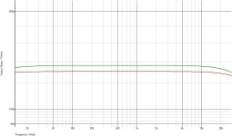
Noise contribution of small values degeneration resistances is negligible anyway, see below the output noise
of a Dual CDV60 amp wich has no degeneration and the influence of two 100R resistances, numbers are
130.5 and 136 nV/sqrt(Hz), that s 0.36B difference.
Attachments
130nV/sqrt(Hz) is nothing to call home about. Thus the additional noise is marginal.of a Dual CDV60 amp wich has no degeneration and the influence of two 100R resistances, numbers are
130.5 and 136 nV/sqrt(Hz), that s 0.36B difference.
Keep in mind that emitter-degeneration is a matter of voltage drop along the degeneration resistors,
so 100R does not tell very much without knowing the emitter current.
Considering op-amps with En<10nV/sqrt(Hz) you won't find emitter degeneration resistors.
I would think that one couldnt say if 130nV/sqrt(Hz) output noise is a lot or not without knowing what is the amp gain,
wich i didnt mention, IPS current is not everything here, yet you made a qualificative estimation without even knowing
a key parameter.
Gain is 18.4, wich amount to 7nV/sqrt(Hz) input noise, better than many opamps, think that the CDV60 date from 1974 or so,
and there s no degeneration in opamps because it is not needed as the transistors are closely matched, if fabrication processes wouldnt had allowed for close matching then they would have added some degeneration as a cure, moreover since opamps have quite low LTP current and that it would have increased noise less than marginaly.
Last edited:

Let's just not throw any more smoke and mirrors
and just listen to Nick S. for once:
"Class ABBA = fine tunend gm-doubling compensation" [Nick] For me, this closes the case once and for all.
kindly,
HBt.

and just listen to Nick S. for once:
"Class ABBA = fine tunend gm-doubling compensation" [Nick] For me, this closes the case once and for all.
kindly,
HBt.
https://www.hifi-wiki.de/index.php/Dual_CDV_60
I love my two old-timers: Dual CV-121 and the ReVox A78 MK II
very nice Amp's 🙂
I love my two old-timers: Dual CV-121 and the ReVox A78 MK II
very nice Amp's 🙂
My previous amplifier in this thread I changed the output with doublecross. 2 pairs biased at 200mA each and one pair biased at 35mA. PSU 45VDC.

Dear @bimo,
would you please show both circuit diagrams - what conclusions have you come to?
thx & greetings,
HBt.
PS
I am amazed at what one can patent.
would you please show both circuit diagrams - what conclusions have you come to?
thx & greetings,
HBt.
PS
I am amazed at what one can patent.
My previous amplifier in this thread I changed the output with doublecross. 2 pairs biased at 200mA each and one pair biased at 35mA. PSU 45VDC.
There s no mention of the bias current in your previous sim, so it s not possible to make any conclusion,
moreover because the subject is precisely OS baising.
"Übernahmeverzerrungen, die Vorspannung und das Kleinsignal-Ersatzschaltbild" - Transfer distortions, the bias voltage and the small-signal equivalent circuit diagram
#
If one summarize the thread and Nick's commercial offer, I state: no gain in knowledge.
That is very disappointing. Since I expect absolutely nothing more in this thread, I'll quietly devote myself to the 25Watt Krill project, which will give me more.
Kits and ideas are a dime a dozen.
kindly,
HBt.
PS
The originator of this thread wants us to follow him on his Paetreon payment account - for me personally, this is diametrically opposed to the DIY community.
Exactly 👍so it s not possible to make any conclusion,
moreover because the subject is precisely OS baising.
and ABBA, the finetuning of gm-doubling-compensation /in Nick Sukhov sense. Perhaps also behind the scenes in the wrangling between book authors, who knows for sure ;-).
The techniques to reduce distortion in class AB are well-known:
* Apply negative feedback.
* Parallel pairs of transistors so that the total bias current is increased.
* Bias the transistors so highly that cut-off occurs only at the highest amplitudes.
Ed
* Apply negative feedback.
* Parallel pairs of transistors so that the total bias current is increased.
* Bias the transistors so highly that cut-off occurs only at the highest amplitudes.
Ed
Would be really interesting to see actual measurements instead of simulation.
The problem with simulation is that each transistor is exactly the same.
This is why wingspread diagrams for parallel transistors pretty much look like for singles.
And this is why cancellation effects can be observed more easily.
In reality, each transistor is slightly different.
This spoils cancellation, but leads to other fortunate effects: The wingspread is flattened significantly with parallel transistors because naturally each has a slightly different crossover point and emitter resistors have tolerance, too.
I wonder whether engineering gm doubling optimization is worth it given it happens naturally in reality?
If you have Kolinummi's book, have a look at figure 7.22 on page 221. He shows measured wingspread.
He shows that with more devices in parallel, wingspread goes to a flat line basically and this is even immune to bias current variation to some extend.
Four transistors in parallel are significantly better than two. Eight are even better, but not that much.
If multiple output transistors are an option, this is the easiest way to linearize a power output stage.
This may even be somewhat cost neutral if lower power transistors are paralleled:
A MJL3281 in TO264 for example costs 4,20€ today (2,60€ for 25). For almost the same money (2,10€ single or 1,25€ for 25) you could buy two 2SC5200N in TO3P.
Bonus is that the thermal resistance of two TO3P is lower than a single TO264.
Assuming you don't spend a fortune for emitter resistors and everything else.
Errata: I was wrong stating the wingspread shows not that much difference for parallel devices in simulation.
Here is a quick simulation of single, dual and quad output devices. 3281 and 1302 with 2R2 base and 0R22 emitter resistors:

For the quad I also added some tolerance to the emitter resistor values, but this doesn't seem to have dramatic effect.
Finding some clever means of flattening gm without parallel devices would be nice though.
Here is a quick simulation of single, dual and quad output devices. 3281 and 1302 with 2R2 base and 0R22 emitter resistors:
For the quad I also added some tolerance to the emitter resistor values, but this doesn't seem to have dramatic effect.
Finding some clever means of flattening gm without parallel devices would be nice though.
Take (also) a look at Nelson Pass
AB100 Amplifier
Four pairs cavort around and form the output stage, not without reason one would think!
AB100 Amplifier
Four pairs cavort around and form the output stage, not without reason one would think!
That's exactly how it is.The consensus seems to be that parallel output transistors are best used to share the load equally.
HBt.
- Home
- Amplifiers
- Solid State
- Class AB vs DoubleCross vs ABBA @ Gm doubling compensation comparison