1K Hz.What frequency and with what amplitude do you put into the input?
The last picture I posted was 10mV p-p.
@BDP
So the definition of the grid would be,
So the definition of the grid would be,
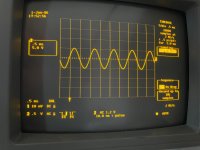
- Every major block on horizontal axis maps to the set time division. In total 10 blocks. Time division set as 0.5 ms, 1 complete period per 2 block, so that would be 1 ms period as I set frequency as 1 kHz. Corresponding.
- The voltage number at lower left of screen would mean voltage difference per block vertically, as I tested different input signal amplitude. Not sure why the voltage division on screen left is 5 V.
Attachments
I agree with BDP. First of all, it is necessary to know what is being measured. And set the oscilloscope time to microseconds. For nanosecond time, you measure MHz.
I agree too. My suspicion goes this direction too actually.it is necessary to know what is being measured
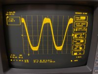
So after a few try setting time interval I was able to get to this.
What I don't quite understand is, I had to turn input up to 900mV to get this stably visible wave, 100mV it would just be a slightly twisting thick band, not readable at all.
I recall CDP and DAC generally do 2.0~2.5V p-p at output, but considering the volume knob resistor on amplifier, I dare not go further much.
I could get an almost sine-looking wave at 1200mV. But on the original paper we don't really turn up input level during front stage testing and tuning.
Attachments
Is the -IN connected to ground? Signal generator connected to unbalanced +IN. Is R81 installed? I think you figured it out. You are measuring noise.
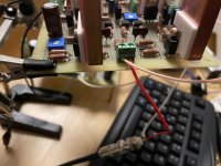
Time to take some well-lit, focused pictures of your setup.
Time to take some well-lit, focused pictures of your setup.
When I first tested the complete amplifier, it oscillated and burned up the RC load resistor and capacitor.
I think that it is not even possible to correctly test and set up the front stage without connected output power transistors. Of course, it must be connected as written by BDP. It is also necessary to set the bias for the output transistors to a minimum - fully open Q11 and then increase the bias. As I already wrote, it is not necessary to connect all power transistors. One pair is enough.
There is one step I am wondering if I missed and was the issue.
In the original paper at very beginning of tuning the 2 trumpets it said (1) check that output offset voltage is low (2) that output is about 2V (AC?) (3) voltage across R7 R8 is around 0.2V.
Now thinking about it output should be AC but I measured in DC, thinking it as output offset voltage.
That is the last thing I am going to try today. The rest has to wait til the chassis parts are sent back to me.
Unless that 2V doesn’t matter anymore once ~0.9V at R7 R8 and low output offset is achieved.
@BDP
Connection is correct as far as I can see.
If R81 is the feedback resistor, no I didn’t install it as it was optional.
I do realized the ns I was measuring is probably some high frequency component. (Or I guess so)
The amp might not be amplifying signal since, well the output doesn’t look amplified.
I think and hope I haven’t broken it, the wave form of empty load looks pretty reasonable and took me no effort to get it on the scope monitor.
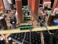
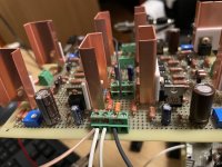
I can get pictures uploaded later, it is barebone minimalist at the moment, just 2 circuit boards.
Did a quick visual check of my front stage, I think I didn't wire components wrong.
To clear up how the front stage behaved.
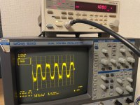
I could get the wave form coming out when I tune R7 R8 down to around 0.2v.
As I tune R7 R8 up towards 0.9V the wave form shrank down to a horizontal line. Just noise, we said.
The wave won't survive past ~0.27V, and looks like a clipped sine wave.
Looks like something is wrong and in a very simple way?
PSU voltage, Z1 Z2 voltage, R9 R10 voltage are correct. DRV+ DRV- voltage ~6.1V.
After reaching 0.9V at R7 R8 and output offset voltage low I can still get the same clipped looking sine wave, just tune signal up to 600mV the wave form will come out.
And I never got 2V AC output.
To clear up how the front stage behaved.
I could get the wave form coming out when I tune R7 R8 down to around 0.2v.
As I tune R7 R8 up towards 0.9V the wave form shrank down to a horizontal line. Just noise, we said.
The wave won't survive past ~0.27V, and looks like a clipped sine wave.
Looks like something is wrong and in a very simple way?
PSU voltage, Z1 Z2 voltage, R9 R10 voltage are correct. DRV+ DRV- voltage ~6.1V.
After reaching 0.9V at R7 R8 and output offset voltage low I can still get the same clipped looking sine wave, just tune signal up to 600mV the wave form will come out.
And I never got 2V AC output.
Attachments
Didn't. I only measured voltage across DRV+ and DRV-.What do you measure with the O-scope at the DRV terminal?
I can try later.
DRV+ and DRV- is the bias voltage for the power transistors. It is set by trimmer P3 - Q11. The voltage DRV+, DRV- is measured against the output - behind the resistor R81.
Power transistors open at a bias of approx. +4V between Gate and S for N channel and -4V between Gate and S for P channel. This pre-voltage is limited by diodes Z3 and Z4 to a maximum of 9V.
If you have this voltage around 2V or less, you can connect power transistors without any worries. Then you can increase the voltage with the trimmer P3. When increasing, measure the voltage on the sensing resistors R34 and R35. For a start, it will be enough to set 0.05V on them. Then you will be able to set the output offset realistically and correctly.
1V on resistors R7 and R8 means a current of 20mA flowing through these resistors. It is DC voltage and current. Do not connect the signal generator to start setting. But connect the terminals IN+ and IN- to GND. It's as if you set the potentiometer at the input to minimum volume.
- Home
- Amplifiers
- Pass Labs
- circuit questions for Pass Thagard A75