I've run into an issue with my oven method of soldering circuit boards. My Chinese PC board silk screen seems to discolour and I think there may be some gassing when it's cooking. Some of the parts are moving dramatically out of place while others are aligning themselves. This is my first attempt at non home etched SMT. I'm going to do some experimenting with lower temperatures and see how it works out.
JW,
Besides the difference in how you are applying the resist to the PCB's vs a commercial process how else is the substrate different? Is it the thickness of the traces that is different or is there something else inherently different that is showing up in this movement of parts in the oven? Have you looked at the precision of your temp control in the oven as a potential problem, I would think with an external controller and a thermocouple you could hold temp very close, much closer than the installed controller in a normal toaster oven. I'm just curious, materials and processing always interests me, so the questions.
Besides the difference in how you are applying the resist to the PCB's vs a commercial process how else is the substrate different? Is it the thickness of the traces that is different or is there something else inherently different that is showing up in this movement of parts in the oven? Have you looked at the precision of your temp control in the oven as a potential problem, I would think with an external controller and a thermocouple you could hold temp very close, much closer than the installed controller in a normal toaster oven. I'm just curious, materials and processing always interests me, so the questions.
My home brew boards are just etched copper with liquid tin applied. Pads are roughly the same size. My Chinese boards have solder mask and silk screen applied. I'm wondering if the solder mask is burping as it's heated? Possibly the extra thickness of the silk is causing the device to seal to the board trapping air, then blowing off when heated. This isn't a huge problem. It's only a few parts. Parts can be realigned quickly enough. The discolouration looks bad though.
Compensation adjustment for different OPS options
Dear friends,
Yesterday Terry had some "burning" issues, testing CF-FET V2.0 with BJT EF3 OPS, loosing four drivers.
I have researched the issue and... it could be avoided if I would do it earlier 🙄
Even for IRFP-based OPS, compensation caps values are slightly different from the initial ones, designed for LFET OPS. With EF3 BJT OPS and original compensation, both gain and phase responses go absolutely crazy. This option requires much deeper compensation. So, the optimal values look like this:
LFET OPS (TubSuMo):
C12, C15: 10pF
C16, C17: 100pF
IRFP-based SlewMasters:
C12, C15: 100pF
C16, C17: 330pF
Original BJT EF3 SlewMasters (and Borys's OPS):
C12, C15: 150pF
C16, C17: 470pF
Although, for IRFP-based OPS initial values are not optimal, but acceptable, for EF3 BJT they are very bad - way too low, leaving the amp at the edge of stability.
I will test/measure the new optimal values for IRFP OPS tomorrow.
I will also copy this info to my CF-FET thread for the benefit of the members visiting that thread.
Terry - many thanks for bringing this up - I hope we all have learned something (or confirmed something we already had a clue about 😉) today
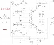
Schematic is attached for your reference.
Cheers,
Valery
Dear friends,
Yesterday Terry had some "burning" issues, testing CF-FET V2.0 with BJT EF3 OPS, loosing four drivers.
I have researched the issue and... it could be avoided if I would do it earlier 🙄
Even for IRFP-based OPS, compensation caps values are slightly different from the initial ones, designed for LFET OPS. With EF3 BJT OPS and original compensation, both gain and phase responses go absolutely crazy. This option requires much deeper compensation. So, the optimal values look like this:
LFET OPS (TubSuMo):
C12, C15: 10pF
C16, C17: 100pF
IRFP-based SlewMasters:
C12, C15: 100pF
C16, C17: 330pF
Original BJT EF3 SlewMasters (and Borys's OPS):
C12, C15: 150pF
C16, C17: 470pF
Although, for IRFP-based OPS initial values are not optimal, but acceptable, for EF3 BJT they are very bad - way too low, leaving the amp at the edge of stability.
I will test/measure the new optimal values for IRFP OPS tomorrow.
I will also copy this info to my CF-FET thread for the benefit of the members visiting that thread.
Terry - many thanks for bringing this up - I hope we all have learned something (or confirmed something we already had a clue about 😉) today
Schematic is attached for your reference.
Cheers,
Valery
Attachments
Hi Valery,
I asked this in the other thread but I'll ask it here for the benefit of those who maybe don't follow that thread. What are the drawbacks to just running the deeper compensation for all three OPS? I'm trying to learn something here.
Thanks, Terry
I asked this in the other thread but I'll ask it here for the benefit of those who maybe don't follow that thread. What are the drawbacks to just running the deeper compensation for all three OPS? I'm trying to learn something here.
Thanks, Terry
Hi Terry,
Sometimes you build faster than I think 😀
Setting these individual values I'm trying to maintain stability, keeping the circuit as fast and wide-bandwidth as possible at the same time, getting the most from it.
Overcompensation will result in more rounded corners on square wave response curves and overall slow-down of the circuit. Although, it would be interesting to see - to what extent, really. Probably, it will still be good.
Cheers,
Valery
OK, if I have them I will swap in the bjt values on one board and test them both with the Tubsumo OPS and see what differences I see on the scope. Then I will stand with fire extinguisher in hand and try the one with the new values with the little bjt ops and see if all is well. 🙂
Thanks again, Terry
Thanks again, Terry
attaching some t/c's and doing a temp profiling might help answer your problem. It could be the sm is just crap too. the assumption is that the sm is lpi type unless specifiedMy home brew boards are just etched copper with liquid tin applied. Pads are roughly the same size. My Chinese boards have solder mask and silk screen applied. I'm wondering if the solder mask is burping as it's heated? Possibly the extra thickness of the silk is causing the device to seal to the board trapping air, then blowing off when heated. This isn't a huge problem. It's only a few parts. Parts can be realigned quickly enough. The discolouration looks bad though.
It might not hurt to contact pcbway and discuss what you are experiencing. They may offer a different solder mask for use in the oven.
Terry
I remember that OS mentioned somwhere about adding extra B-C caps at the drivers but I do not remember for which ones. For safety You can try to put 100pF cap on each driver in small BJT ops board.
Valery
What would You think ?
THX
I remember that OS mentioned somwhere about adding extra B-C caps at the drivers but I do not remember for which ones. For safety You can try to put 100pF cap on each driver in small BJT ops board.
Valery
What would You think ?
THX
When I get some time I'll try it again with a little neater paste application and temperature control. I don't think I need to go nearly as warm as I am to reflow with the solder I'm using but Chip-Quik isn't the best at releasing any data on their products.
I'm going to check into higher temp silk screen too.
I'm going to check into higher temp silk screen too.
Terry
I remember that OS mentioned somwhere about adding extra B-C caps at the drivers but I do not remember for which ones. For safety You can try to put 100pF cap on each driver in small BJT ops board.
Valery
What would You think ?
THX
Yes, sometimes it helps. However, in most cases some 47pF at the pre-drivers are enough to control the local stability... worth testing though.
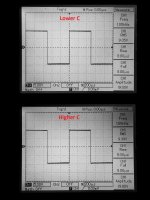
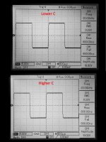
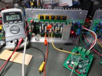
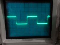
OK, tested the higher compensation with the TH version of the front-end (just easier to change the caps).
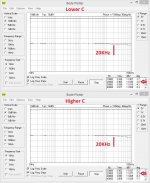
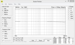
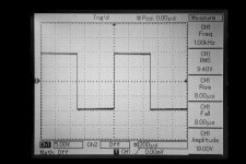
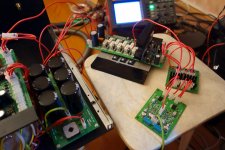
OPS is IRFP-based. Input filter is in place, Zobel/Thiele network is in place. The load is 8R.
Lower C values: C12, C15 = 10pF; C16, C17 = 100pF
Higher C values: C12, C15 = 100pF; C16, C17 = 330pF
1-st picture - the whole test setup;
2-nd picture - 1KHz square wave response;
3-rd picture - 20 KHz square wave response;
4-th picture - measured Bode plots.
As we can see, it still looks good with deeper compensation, however it's got better stability margins. So, I leave it this way, with the higher C values.
Cheers,
Valery
Attachments

Well I checked and I don't have the 150p in smd. I'll have to order some. I suppose I could try the 100p/330p and see how that goes. I do have them in through hole so I guess I could try with the through hole version first.
Blessings, Terry
Blessings, Terry
For BJT OPS 150p/470p is safer. You can actually try to carefully solder TH caps on SMD pads for a test.
Hi Valery,
I know this is probably your sleep time. I just change the caps to 100p/330p. I hooked it up to the Vfet ops. First issue is bias. With the bias adjusted all the way down I have 74V across a pair of 0R22 emitters. That's almost 170mA. Too high for my needs. Next is the square wave. Some weird looking over shoot. Puzzling that I am using your values in my OPS yet we get such different results. I'm attaching pics for your evaluation.
BTW, both boards do exactly the same thing through either OPS.
Thanks, Terry
Attachments
- Status
- Not open for further replies.
- Home
- Amplifiers
- Solid State
- CF-FET V2.0 front-end - going high-tech (SMD)