I love the OS-CON caps, but for me, the Nichicon FP polymer series also sounds lovely in my systems that I applied it.Many thanks for the feedback (and PM advices also : much appreciated).
I checked through hole Sanyo Os Con catalog and don't find 1200 uF/16V. My prefered are the SEP serie that has not such high capacitance. When I look at SEPC/F the max is 1000 uF and are 10 mm diameter as the footprints I chose (with a margin to 12 mm diameter spacing on the pcb and double spacing gap for the TPH in order some diyers can choose their own. I disllike a lot the SEPC/F I plenty have but found they sound zingy when used in an anlog DAC supply (pin 15, or else PCM dac ics I tried : AD1862, etc)
So, beyond the excellent ESR of the OSC CON, I find the new ones not sounding as good as the NLA formers and for my tastes till now, mostly for the -15V (so here I put a margin for bigger caps and double leads pitch gap : 5mm + 7mm). Of course, on must hear your design with the BOM as it was simed like that and the tricks you use are subtles and based too on listening long experience (that matterd a lot in my agenda : I bougth the first microIdsd from Ifi but couldn't affoard CD77 from AMR). ANyway I found the SEP serie the best of all the new oscons ! Because darker and less zingy (barely soft at the opposit of the SEPC/F) if not at all, but I don't like polymer in analog decoupling but another brand model (I literraly tried all the new polymers models and brans for my former TDA DAC Audial core based and the winner wasnot an os-con : whatever they have same esr & inductance at iso capacitance/voltage : the do NOT sounds the same too me, whatever I repeat the tests. BUT and it is a huge one, it was not tested in a shunt PS !
What the assymetry you are talking about please ? SMA pads ? Tracks on top layer ? Else ? : power side ( the many island on insides layers make it the topsymetry for eyes difficult but I can try better)?
For the tracks, the minimum spacing I use is the text book x3 width spacing (used for flip flops vinicity for illlustration). On the longer tracks FDEM, AoL/R, assymetry was a question of spacing with some signal vias, or to break too long // Tracks for antena coupling despite the spacing here is huge already (no needs of via fencing walls for instance). Sometimes I used assymetry to avoid things like M4 through hole in a corner (WRclk uf-l) or to make shorter the tracks for Mclk and FEDEM_Bck : but that's my french Cartesian side 😉 : in practice it certainly is not mandatory, so I can align (I do like too it looks good 🙂 )
As I send you a pcb, I'd like you find it looking good too 😊 !
Edit : I'm planning something in order you use the Super caps option you prefer. I willl use this pcb above cause the super caps are a little expensive for my own needs).
The TL431 caps are 10 mm diameter foot print, so caps could breath with all the close heat : double space leads gap here : 5mm and 2.5 mm 😉
(here btw my experience is the Pani FR are f....g good but according the smoothing caps chosen before; Pan FM here, nope; Pan FC yes or not (they are very clear and neutral : my ref to swap a sepc/f on analog sides)
What is the spacing of the Super caps you use, please in order I check the footprints needed.
cheers
I didn't like the FP. They can have that smooth sweet sugary character of the new OSCON SEP if such words makes sense !
No it is not... Just marked red lines in relation to n x Fs. But without frequency?
Ohhh, ok, my bad. I thought you were interested in the SINC envelope, not in the frequency of the image os a single time.
It's mirrored around FS, with a minimum at FS.
If FS = 44.1kHz and the single tone is 1kHs, the the image appears at 44
1kHz - 1kHz or 43.1kHz.
For (say) an equal mix of 19kHz and 20kHz images appear at 24.1kHz (image of 20k) 25.1kHz (image of 19kHz).
For (say) a 100Hz tone, the image appears at 44kHz.
Level of a given frequency image follows SINC plus any additional filtering.
Thor
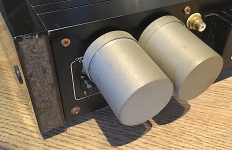
AMR Diablo dac . . .
View attachment 1373548
The "iFi Diablo" was codenamed "red label" . . . .
Thor
The picture does not do justice to the VERY exclusive & futuristic enclosure design.
What was visible through the top plate revealed an absolutely no-compromise approach to oscillator design & distribution.
What a shame . . . It would've been a reference design to follow . . . . Alas it was never released.
@thorsten:
What DAC chips did you use in this dac??
Last edited:
@ThorstenL and @Zoran ,
I'd like to make a pcbof each of what you consider the Solid State circuitry you would prefer for yourselves (I have just a single ECC188, so complew I/V stages with several tubes is out of my scope), to try both.
As I will pass an order to JLCP to test my design for real, I can make a one bill to save on shippment.
Can you send me please the diyaudio link if your posst about that among the several you published (for the core pcb I take always the last one from Thorsten).
I can off course send you a pcb as the minimum MOQ is 5 pcbs !
But I can also test it with for instance the opa861 stage of P Rogic I find good with the good decoupling caps (the Eldam mod).
Let me know if interrested by PM.
Pat diGiacomo told me about the AD1862. If you are in the "testing phase" make sure you have anti-parallel diodes protecting the output. Even operating it open, nothing connected, can damage the chip. Beware of turn-on and turn-off transients of whatever is connected to the outputs.Or simply just an I/V with very low impedance input BJT (output impedance TDA 1541A that high ???) as the discussed shematic has a lot of pins filtering ? Jfet seems out cause unconcistancy (T.'s input sooner inthe thread)
By the way I wonder if the outputs of the TDA1541A are not internaly protected by diodes or somewhat ? I know AD1862 hasn't, @Alexandre reported about that last chip times ago.
For maximum resolution you may want to remove the diodes, after everything is validated. Especially when using resistor I/V.
Last edited:


Yes but in any case i think that 2 x parallel opposite fast diodes. should be attached at the output. Closer to the chip.By the way I wonder if the outputs of the TDA1541A are not internaly protected by diodes or somewhat ?
(IV conversion, if it is with simple R, should be closer to amplifying circuit next Riv...).
Current injection 2mA, also closer to the chip.
I made it with formulas and with functions plots. To make it more familiar with.Ohhh, ok, my bad. I thought you were interested in the SINC envelope, not in the frequency of the image os a single time.
It's mirrored around FS, with a minimum at FS.
If FS = 44.1kHz and the single tone is 1kHs, the the image appears at 44
1kHz - 1kHz or 43.1kHz.
For (say) an equal mix of 19kHz and 20kHz images appear at 24.1kHz (image of 20k) 25.1kHz (image of 19kHz).
For (say) a 100Hz tone, the image appears at 44kHz.
Level of a given frequency image follows SINC plus any additional filtering.
Thor
There are some mirror "images" related to Fs rate and Bit length.
.
I attached PDF file of MatCad .MCD sheet too. If somebody wants .MCD file please ask.
Attachments
Every diskrete IV showed in this topic is more than OK at least in the sims from my perspective. And I almost 100% know that they will perform better than with OPs.@ThorstenL and @Zoran ,
I'd like to make a pcbof each of what you consider the Solid State circuitry you would prefer for yourselves (I have just a single ECC188, so complew I/V stages with several tubes is out of my scope), to try both.
As I will pass an order to JLCP to test my design for real, I can make a one bill to save on shippment.
Can you send me please the diyaudio link if your posst about that among the several you published (for the core pcb I take always the last one from Thorsten).
I can off course send you a pcb as the minimum MOQ is 5 pcbs !
But I can also test it with for instance the opa861 stage of P Rogic I find good with the good decoupling caps (the Eldam mod).
Let me know if interrested by PM.
.
I will take a look at the ECC188
I tried that discrete IV on the veroboard it performs quite good in both measurements and sound. H2 was -85-90db.Every diskrete IV showed in this topic is more than OK at least in the sims from my perspective. And I almost 100% know that they will perform better than with OPs.
Here is what i tried:
I did it without sallen-key filter for the start. Just 1st order (C2). R2 is indeed 1.21k
Hi there is no link to the pic?Here is what i tried:
Thanks 🙂
...
Sorry there was some glitch, picture appeared on click...
Thanks
Last edited:
I didnt find ECC188 datas so I used E188CC datasheets from Siemens and Philips.
3 spice models .INC files are In the Zip folder. Almost the same...
.
there are few solutions to use this tube. Pretty much the same as ECC/PCC88.
.
1.
Standard Amplification stage with Riv=22 ohm, output in phase, 12K load, 1.5V battery biasing (or RC), about 2Vrms output, Zout=2,2K, two sections im parallel (and load too...) 1.1K Zout... Very low distortion.
2.
Grounded grid, with JFET, sch was in topic before, very small THD, very good PSRR, simple... Also parallel sections with 2 x JFET
3.
SRPP, parallel sections, with EL84 as the load in triode mode.
4.
MJU follower, parallel sections, with EL84 as load.
...
Paralleled sections because of the lower Ri, higher transconductance and Screen and cross sections capacitances. That is the pretty much standard tube, produced in large quantities, so from the same bunch specimens are identical... Probably wider...
.
I will post some schematisc.
Attachments
Last edited:
Lots of great ideas.Every diskrete IV showed in this topic is more than OK at least in the sims from my perspective. And I almost 100% know that they will perform better than with OPs.
.
I will take a look at the ECC188
Keep up the good work 👍
Tips:
Make sure the I/V stage is capable of resolving at least 16 bits.
Tube-based or transformer cpl:ed stages cannot resolve 16 bit from 20-20 kHz:
Attachments
Tube-based or transformer cpl:ed stages cannot resolve 16 bit from 20-20 kHz:
This example https://www.bramjacobse.nl/wordpress/?p=6233 is the wrong one ( also use by Thorsen to discredit trafos , that he doens't know about )
trafos works great ( better than active I/V , sound wise ) when they are correctly implemented , you have here some examples 😉
This is also what said John Brown from ECdesign ( with a lot of experiences , not just words ) , even if lately some here seems to forget the quality of it's contribution to the matter , especialy in the real world , the one I Iike and prefer 😎
.
Last edited:
Hi Fabrice
I take it that you've gain success with trafo i/v, care to share your thoughts & experiences ?
Thks
I take it that you've gain success with trafo i/v, care to share your thoughts & experiences ?
Thks
Some 2 cents or so about trafos/tubes...
Trafo have "voltage gain" (=voltage step-up, impedance converting) with less Johnson noise than perhaps every ampop ever devised by mankind. Laws of physics. Of course, the challenge is about the mains noise induction. Good magnetic shielding and orientation works wonder here.
Trafos will not maintain zero ohm in the primary to MHz range, but is only a matter to implement as a part of filtering, a cap in the primary side, or even some CLC previous to it. Like the small cap (SMD) direct from the DAC out, for glitch control, as Thorsten pointed out. If anyone are concerned with the HF loading of the DAC out.
With tubes, with proper implementation, is possible to discern in a 16-bit DAC about it being feed by a 24 bits dithered to 16 bits, or being feed by a 24 bits truncated to 16 bits. Of course, noise always be higher than the silicon counterparts, no contest about it, being far from 24 bits, anyway. But for me the SN/R of tubes always suffices using analog volume control in the amps/pre. Will be bothersome only if one connect it directly to a eg. 2kW amp with high gain, controlling volume digitally.
Hi Fabrice
I take it that you've gain success with trafo i/v, care to share your thoughts & experiences ?
Thks
The credit goes to John , I followed hes advice carefully and it's a long way to read and go , nothing fancy here but a great care of any minimum details , lipo battery power is an great help in the overall result
.
- Home
- Source & Line
- Digital Line Level
- Building the ultimate NOS DAC using TDA1541A