I have these Chinese CPLD boards, so yes, I expect to use simultaneous mode. Not because it's magic (correct input signal conditioning is the "magic") buit to get 384kHz capability.
Thor
Ok, so you had not the time to check if the sim mode programation (datasheet) is working with the new pins routing.
Indeed no magic but the only way to get 384 K hz. Also it has more resolution also in NOS mode, certainly because speed divided per two or maybe what happens inside the chips ! I dunno. Difference are obvious, and more with late Taiwanns I found (in my setup at least : 15 bits stop clock s sim mode from the 1.1 I2S to PCM from IanCanada, slaved by a MasterClock (Crystek or Laptech SC-Cut)... non upsampled in my setup.
I am looking forward to know if that works with the new pins alocations about the sim mode according how it is made on the original datasheet (pin 26 to 28)
Last edited:

Certainly needs a reclock after... or maybe slaved already ?In case you are thinking of a nos/os system, I could make my latest Saa7220 pin compatible work available to the community. It features CPLD technology with code written by @miro1360 .
I wondeered about the SAA7030 chip to adds two artificial bits to the TDA1541A ! Although shouldn't work as made for a 14 bits dac chips (TDA1540) : not the same timing about Lr edge start position, etc ! Above my head !
Last edited:
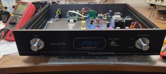
In reality I would also have the entire PCB of a dac project with tda1541 conceived in a "modular" way ,on It ,with small modifications other dac chips could also be used for example ad1862 (but here we are talking about tda1541), or also with the possibility of change the only i/v converter output stage. At the moment I am on holiday, but I always read you with great pleasure, I will attach the files as soon as I can. I am now attaching the photo of the DAC with tube output.
Many thanks to @miro1360
I apologize in advance for my English.
Many thanks to @miro1360
I apologize in advance for my English.
Attachments
-
 IMG_20240503_210149.jpg261.6 KB · Views: 124
 -
 IMG_20240503_210113.jpg312.3 KB · Views: 124
 -
 IMG_20240503_210036.jpg323.6 KB · Views: 126
 -
 IMG_20240503_122725.jpg333.7 KB · Views: 132
 -
 IMG_20240503_122718.jpg289.1 KB · Views: 136
 -
 IMG_20240502_212123.jpg242.2 KB · Views: 127
 -
 IMG_20240502_212108.jpg258.8 KB · Views: 111
Unfortunately I can't answer you... but I know that Miro is working on an update to the code regarding the re clock... so if you have any questions it's best to ask him directly, he's a very good and helpful person.Certainly needs a reclock after... or maybe slaved already ?
I wondeered about the SAA7030 chip to adds two artificial bits to the TDA1541A ! Although shouldn't work as made for a 14 bits dac chips (TDA1540) : not the same timing about Lr edge start position, etc ! Above my head !
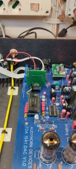
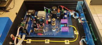
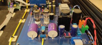
Some things strange to me on the blue board . Congrats for the tiny green cpld layout 🙂 .
Blue board : 12AX7 tempting for the high Mu as I/V but chineese or russian made nowadays ????
Black holko metal film : good if the NOS ones (not the nowadays remade)
RN55 resistors : a pita : it dulls and smooths everything, as a strong spice as to be used with a lot of care or it kills music. Do use RN60 instead. (or Yageo 0.1%)
Clarity Cap CSA : can be good or not related to wht is outputings : The MR & CMR are verry neutral and way better but the price ?! I like Tin foil from SCR here or MIT RTX (NLA).
Are the cab with blue K from Kemet or ???? The Reds are Wurth ? (no experience with them); but the blue alumin canned polymer very differ from brand to brand.
And I do not say it sounds bad : equilibrium between parts choice and layout is something strange as it is related IME with how is sounding the rest of the hifi devices... But when the sources is precise and neutral it is easily showing the rest of the hifi devices + room choices...
I have to test it for my TDA 1540s' 🙂Unfortunately I can't answer you... but I know that Miro is working on an update to the code regarding the re clock... so if you have any questions it's best to ask him directly, he's a very good and helpful person.
Ok, so you had not the time to check if the sim mode programation (datasheet) is working with the new pins routing.
There is no "new pin routing".
All that changes is how precisely we decouple pins.
The standard methode links both grounds and decopuples everything to ADND/DGND which we know causes problems.
The difference between taking a non-polar DEM capacitor directly to -15V instead of taking it to AGND where the current then must return to -15V via the AGND to -15V power supply is subtle. It doesn't change actual operation, just where unwanted noise ends up dumped to.
Now the specific input mode you select simply determines how the input latches forming the input shift register load data from input pins. That's basic logic. It of course remains unchanged.
Indeed no magic but the only way to get 384 K hz. Also it has more resolution also in NOS mode, certainly because speed divided per two or maybe what happens inside the chips ! I dunno. Difference are obvious, and more with late Taiwanns I found (in my setup at least : 15 bits stop clock s sim mode from the 1.1 I2S to PCM from IanCanada, slaved by a MasterClock (Crystek or Laptech SC-Cut)... non upsampled in my setup.
Lots of magic incantations.
Have you applied signal conditioning to the various signals?
I am looking forward to know if that works with the new pins alocations about the sim mode according how it is made on the original datasheet (pin 26 to 28)
There is no change to functionality at all. Link pin 27 to 26 to set SIM mode, connect the correct pins.
Most important, limit the slew rate of the input signals, to not exceed the slew rate of the PNP input transistors and limit the voltage swing to little enough to not drive the input differential pair into cutoff.
Do this and all noise difference between IIS and simultaneous mode disappear, because the noise disappears, as the source that caused the noise to appear is deactivated.
Thor
PS, Actually all I'm discussing is about minimising noise sources on the TDA1541 as well as anything causing HD. And I am looking to do it in a fundamental way, ground up, not using hacks or workarounds.
Very good to see this old thread come to life.. . . Actually all I'm discussing is about minimising noise sources on the TDA1541 as well as anything causing HD. And I am looking to do it in a fundamental way, ground up, not using hacks or workarounds.
I don't think I've ever read the inner workings of the TDA154xx chip explained as clearly as mentioned above.And Again - Decoding TDA1541 Power and Ground Pin's, the definitive edition. . . #9,012
Wish I had this info 30 years ago.
👍 to TL
Anything analogue must be star-grounded (returned) to -15V, NOT AGND.
While this DOES include the analogue output current, this cannot be done directly.
The AOL/AOR pins need to be kept at < +/-75mV (preferred < +/-25mV) difference from the AGND pin.
The current then must somehow pass through the current to voltage conversion resistor to give output voltage and then return to -15V.
If (say) using an Op-Amp I/U converter, the Op-Amp keeps the inverting input at "AGND", the signal current must flow through the feedback resistor, which is the actual I/U conversion resistor. The current then flows into Op-Amp output and from there to the relevant PSU pin of the Op-Amp.
Obviously the +V powersupply and -V powersupply ONLY of the I/U conversion Op-Amp should be shared with the TDA1541 (yes, +5V and -15V!). This suffices for 2V RMS using modern OPA's. By sharing the power supplies all current loops are shared.
A genuine TI OPA2156 from Mouser (too many fake OPA1656 out there) is an excellent choice here and makes a VERY credible I/U converter with good sound using TDA1541.
A servo Op-Amp should be used to control a CCS from +5V to AOL/AOR, drawing around 2mA and servo adjusted to "null" the I/U conversion output.
Active or passive filters can then follow without extra DC blocking. Other options have been discussed in this thread.
Thor
There is no change to functionality at all. Link pin 27 to 26 to set SIM mode, connect the correct pins.
Most important, limit the slew rate of the input signals, to not exceed the slew rate of the PNP input transistors and limit the voltage swing to little enough to not drive the input differential pair into cutoff.
Do this and all noise difference between IIS and simultaneous mode disappear, because the noise disappears, as the source that caused the noise to appear is deactivated.
Thor
PS, Actually all I'm discussing is about minimising noise sources on the TDA1541 as well as anything causing HD. And I am looking to do it in a fundamental way, ground up, not using hacks or workarounds.
Thanks, I was not confortable with that as 26 was not feeded from outside anymore.
Thanks, I was not confortable with that as 26 was not feeded from outside anymore.
Of course pin 26 is fed from the outside. It has to. It still wants -5V @ 45mA.
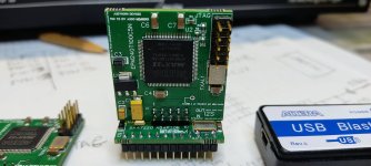
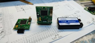
Oh my God...difficult for me to answer all these questions...it must have been at least 3 years since I finished this project, many of the components I usually have in my drawers and I have therefore used them, some others I took from Mouser...I do not produce to sell, what you see is my only example in my possession. I also developed Saa7220 to CPLD module to achieve both nos and simultaneous mode. I have another release with the ability to change both the DAC chip and the output stage, but I haven't realized it yet and that's all for now.😊Some things strange to me on the blue board . Congrats for the tiny green cpld layout 🙂 .
Blue board : 12AX7 tempting for the high Mu as I/V but chineese or russian made nowadays ????
Black holko metal film : good if the NOS ones (not the nowadays remade)
RN55 resistors : a pita : it dulls and smooths everything, as a strong spice as to be used with a lot of care or it kills music. Do use RN60 instead. (or Yageo 0.1%)
Clarity Cap CSA : can be good or not related to wht is outputings : The MR & CMR are verry neutral and way better but the price ?! I like Tin foil from SCR here or MIT RTX (NLA).
Are the cab with blue K from Kemet or ???? The Reds are Wurth ? (no experience with them); but the blue alumin canned polymer very differ from brand to brand.
And I do not say it sounds bad : equilibrium between parts choice and layout is something strange as it is related IME with how is sounding the rest of the hifi devices... But when the sources is precise and neutral it is easily showing the rest of the hifi devices + room choices...
That'd be cool for sure!In case you are thinking of a nos/os system, I could make my latest Saa7220 pin compatible work available to the community. It features CPLD technology with code written by @miro1360 .
Thanks.MPSA18 are very high beta, low noise audio transistors. The trick is the high beta. Typically 1100 @ 1mA IC with 160MHz gainbandwidthproduct.
Wish there was an equivalent PNP. Now that our main control transistor is PNP (as we fold over to -15V reference.
Thor
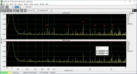
Perhaps better visible on this magnified FFT spectrum. The fundamental is 437.875 Hz. The 1 kHz and multiple peaks are probably due to the digital generator, ignore them. I haven't implemented the input signal conditioning yet, I am curious what improvement it brings.... where are the harmonics onthe graphs, please ? Are they the main peaks with overshoots in betweens (the small peaks) ?
Attachments
Obviously the +V powersupply and -V powersupply ONLY of the I/U conversion Op-Amp should be shared with the TDA1541 (yes, +5V and -15V!). This suffices for 2V RMS using modern OPA's. By sharing the power supplies all current loops are shared.
A genuine TI OPA2156 from Mouser (too many fake OPA1656 out there) is an excellent choice here and makes a VERY credible I/U converter with good sound using TDA1541.
Thor
Hello,
I finisheed with the opa861 with its 7R input and not virtual R I/V. (Pedja's). Surely needs the good PS related to TDA1541A 110 dB SNR, not as hard PS as you highligthed before (although always should have some virtues : low impedance, etc). Sounds good to me if efforts made around with PS and passive parts.
There are plenty of op amps that seems to performs better tha the 2156. Here te differential input R is "high" and settling time so-so. Okay THD, etc looks good, but plenty of opamps are ok here too and better on the paper. Although the fab qualities had improved... Opa1656 has not specialy good specs VS opa861, AD711 (and LME49713HA), opa820, opa 838, AD4899, op656, opa1633 (I really needs to try this one despite its High Z input), etc
But this is not my question. I haven't understood the shared PS related to the +5V and -15V input . Does it mean that the op amps should be PS feeded from these TDA1541a rails ? With classic VFB, I try to make the gnd of the lythic and decoupling very ear each others and towards the output of the VFB op amps as you highligthed. But not sure I understand shared +5V/--15V and the shared loops but the Agnd (hatever the new and old) to be from the party with the signal output (finally the +5V for the current output of the TDA1541A). What is worrying me (but frankly way above my basic knowledge, though I listened tons of DACs) is finally all of this analog current loops at the end now are going to different loops for the analog side (-15V and +5V). For the op amps which one is the more anallog ? It seems it is +5V ?
But anyway sterile discuss certainly, the discrete seemss to be better because more versatile to design. I reaaly want to try all the goods I/V that poped up from few pages. Just that Ground loop thing is what I do not understood from your input (shared (+5V/-15V related to the rails of the op amps and/or if discrete design).
Last edited:
There are plenty of op amps that seems to performs better.
Op-Amp's operate differently to a transimpedance amp (aka current conveyor).
Here te differential input R is "high". Okay THD, etc looks good, but plenty of opamps are ok here.
The circuit must be understood.
Look at the TDA1541. Per channel we have two digitally controlled, complementary current SINKS with 2mA centre current, one connected to +5V and the other to "output".
Let's now connect a 1.5k resistor from Output to Ground. This gives us theoretically ~2v rms out.
But that does not work. The TDA1541 output voltage compliance does not allow this.
So, let us introduce a "servo".
The reference input of the servo is connected to AGND, the feedback input of the servo is connected to the TDA1541 output and the servo output is connected to "far" side of our 1.5k current to voltage resistor.
Our servo now applies voltage to the Resistor that keeps the feedback input and TDA1541 output at the same potential as AGND.
The output will move to keep the feedback input at zero, within precision and speed limits (any servo is an integrator).
The current from our current sink inside the TDA1541 still flows through our 1.5k resistor. The Servo output will need to absorb the current flowing in the 1.5k resistor. This current should return to the +5V rail, because it cancels out the AC component of output current directed to the +5V rail, the sum of both currents being 4mA DC. At this point the decoupling from +5V to -15V lacks any signal related components.
IF we use a differential amplifier to pick up the voltage across our 1.5k resistor, we still have completely passive I/U conversion and we ignore the errors of our servo. Our servo only keeps the TAD1541 output within the voltage compliance range. Errors caused by servo appear at TDA1541 output and as a result on the servo-output.
Our differential amplifier only amplifies the voltage across the 1.5k resistor and gives a true voltage representation of the TDA1541 current. A transformer is also a differential device, incidentally.
Of course, this doesn't quite work in reality.
If we use OPA2156 as "servo" we can use a 1k I/U conversion resistor, but not 1.5k.
So it doesn't make a working I/U circuit quite like this.
Most people combine Servo and Differential Amplifier and pick the signal from the "servo" output, presuming all errors are sufficiently small.
I haven't understood the shared PS related to the +5V and -15V. Does it mean that the op amps should be PS feeded fro these TDA1541a rails ?
If using classing I/U conversion, Yes. And we should not compensate the offset current.
We can put a servo elsewhere.
With classic VFB, I try to make the gnd of the lythic and decoupling very ear each others and towards the output of the VFB op amps as you highligthed. But not sure I understand shared +5V/--15V and the shared loops but the Agnd (hatever the new and old) to be from the party with the signal output (finally the +5V for the current output of the TDA1541A). What is worrying me (but frankly way above my basic knowledge) is finally all of this analog current loop now are going to different loops for the analog side (-15V
Draw out the circuit...
Here I show an external pass transistor and CCS added to an Op-Amp (say NJM2068).
Signal currents in the TDA1541 originate at -15V and are split into variable currents, one of which is sent to +5V and the other to out and the sum of these two currents is 4mA.
If we do not send the signal current to +5V, but elsewhere (e.g. separate +15V), this current needs to return to somewhere where we also send the current from +5V, via imperfect supply decoupling capacitors.
Ultimately the two split currents need to reunite and flow as DC into the -15V pin.
Thor
- Home
- Source & Line
- Digital Line Level
- Building the ultimate NOS DAC using TDA1541A