A J-Fet is, like a Tube and a Depletion Mosfet "self-biasing".
So it becomes a 2-terminal device.
All current sources shown with a reference input (they are all "non-feedback" types and it would be possible to make them feedback types) ultimately operate by imposing the reference voltage (minus the BE voltage of the transistor) across a resistor.
It is noise and stability of this voltage that determines noise and stability of the current.
Ultimately, the PNP -BJT option all have a current "sourced" from +5V and and [assing to -15V from the power supply closes the current loop to +5V.
The "reference side chain" should also connect to -15V. There is a that I made a 20V power supply, not 5V.

Additionally, when it comes to various current sources, the late but great Walt Jung did a lot of work on this, which can be found here:
Click to read the article - Part 1: Basics of Operation
Click to read the article - Part 2: Precise High Current/Voltage Operation
Click to read the article - Letters and Addendum
Thor
So it becomes a 2-terminal device.
All current sources shown with a reference input (they are all "non-feedback" types and it would be possible to make them feedback types) ultimately operate by imposing the reference voltage (minus the BE voltage of the transistor) across a resistor.
It is noise and stability of this voltage that determines noise and stability of the current.
Ultimately, the PNP -BJT option all have a current "sourced" from +5V and and [assing to -15V from the power supply closes the current loop to +5V.
The "reference side chain" should also connect to -15V. There is a that I made a 20V power supply, not 5V.
Additionally, when it comes to various current sources, the late but great Walt Jung did a lot of work on this, which can be found here:
Click to read the article - Part 1: Basics of Operation
Click to read the article - Part 2: Precise High Current/Voltage Operation
Click to read the article - Letters and Addendum
Thor
The Walt Jung material was great but I couldn't find it... having used numerous implementations myself. Glad to see you found it Thor. I still like the CCS implementation with a collector attached to the In+ just to keep the capacitance low.
Yes, it is a ~440 Hz 0 dBFS digitally generated sine with dither. Note the 0.001% THD at "optimal" conditions, I/V converter (NE5534) included.A 0dBFS signal at 450Hz?
What is the "reference" circuit and what is the circuit where the I/U conversion resistor is varied (without apparently varying the levels)?
The variable resistor was inserted between the TDA1541A analog current output and the inverting input of the NE5534. This is not the actual I/V resistor, that is 1.5k in the NE5534 feedback loop. The variable resistor just disconnects the TDA output from the virtual ground and elevates its voltage according to the analog output current. For example at 4 mA positive peak current and 33 ohms the voltage at the analog current output is 132 mV. It is beyond the data sheet permitted 25 mV, which is probably a little conservative.
Some of you might already know. The owner of https://www.mvaudiolabs.com/ is actually a member here. His diyaudio profile is sampler.
Been some time since he visited diyaudio
Been some time since he visited diyaudio
The -2mA should flow towards the analog current output, so we need a positive voltage and a CCS. A resistor from +5V or +15V, or a jFET with a current adjusting resistor between G-S will do. I used 2N3819.Maybe the 2mA current should be point to -15V? As pure amalog?
Here you go. 68R resistor, -2mA CCS. Compare the upper (L) trace that is default, with the lower (R) trace tested.Sadly your test cuts of at H4 so we cannot evaluate H5 - H10.
Attachments
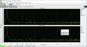

Great to see some real world results. Gives me something to compare with.Here you go. 68R resistor, -2mA CCS. Compare the upper (L) trace that is default, with the lower (R) trace tested.
Yes, I meant like that (with R4 conn. to "-15V" instead of "GND"), for that way of CCS.
And I think that some slight better results are with diode made from BJT, forming an Current mirror in that part of circuit. I simulated this and posted before...
.
Why are you transferred to BC337/BC327 from MPSA18? 🤢
Yes, it is a ~440 Hz 0 dBFS digitally generated sine with dither. Note the 0.001% THD at "optimal" conditions, I/V converter (NE5534) included.
Thank you for the clarification.
It is beyond the data sheet permitted 25 mV, which is probably a little conservative.
The 25mV (50mV PP) suggests 12.5 Ohm.
If you look at MVAL's results there are three "knees", at around 35 Ohm, near 10 Ohm and below 5 Ohm.
Above 35 Ohm HD rises quickly, H2 dominant, exceeding 0.1% (H2 dominant) at around 68R.
We then see a "plateau" down towards 10R (especially H2, H5) before we see harmonics drop away again.
Thor
Are you sure about this?
Now you mention it, I am sure about Walt Jung and Great.
It seems I jumped the gun on him shuffling of this mortal coil as he kinda dropped out view at a time when old engineers dropped like flies. May he live long and prosper.
Well, "Two out of three ain't bad".
Thor
And I think that some slight better results are with diode made from BJT, forming an Current mirror in that part of circuit.
Yes, but more complexity. A 3V3 Zener has nearly the same negative Tempco as a BJT, so we get sufficiently stable current with temperature for my final circuit. Adding 1k/1,000uF is really being extreme on noise. I might drop it.
A 3V3 Zener has 70 Ohm impedance and produces around 1uV Noise. Without any filtering, with 470R we get 2.12nA noise current, compared to 4mA PP signal, or around -116dB.
Why are you transferred to BC337/BC327 from MPSA18? 🤢
MPSA18, no improvement and I have spare327/337.
MPSA18 or SS9014 is not a big deal. Finally 2N3904 is faster.
Thor
I have MPSA18, 🙁 at hands, will try it, but off-course other types that You point at, thanks.MPSA18, no improvement and I have spare327/337.
Also I will post some other circuits taht types that I was playing around earlier, same "concept" - to put the circuit in "opposite" way at the -15V side 🙂
Here you go. 68R resistor, -2mA CCS. Compare the upper (L) trace that is default, with the lower (R) trace tested.
Thanks Icazar,
For the basic people like I am, where are the harmonics onthe graphs, please ? Are they the main peaks with overshoots in betweens (the small peaks) ?
Whzn I read 48 Khz /24 bits, is it the resolution you chose for the sound card or the one of the signal injected, please ?
On MV audiolab the good choice to have odd Harmonics a little lower seems to be 35 to 38R after 40R H3 seems to land off as a rockett. The 50R with low H5 is a trap at seing H3 !
Sorry for the digress.
@ThorstenL, do you use the new voltage lines and new pins to put the TDA1541A in simultaneous mode or the ancient pins ? Sorry, certinly a naive question.
I have MPSA18, 🙁 at hands, will try it,
MPSA18 are very high beta, low noise audio transistors. The trick is the high beta. Typically 1100 @ 1mA IC with 160MHz gainbandwidthproduct.
Wish there was an equivalent PNP. Now that our main control transistor is PNP (as we fold over to -15V reference.
Thor
@ThorstenL, do you use the new voltage lines and new pins to put the TDA1541A in simultaneous mode or the ancient pins ? Sorry, certinly a naive question.
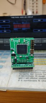
I have these Chinese CPLD boards, so yes, I expect to use simultaneous mode. Not because it's magic (correct input signal conditioning is the "magic") buit to get 384kHz capability.
Thor
Thanks Icazar,
For the basic people like I am, where are the harmonics onthe graphs, please ? Are they the main peaks with overshoots in betweens (the small peaks) ?
The harmonics are the multiples of 440 Hz, and you are right, they are the main peaks (880 Hz 2nd, 1320 Hz 3rd, 2200 Hz 5th)
Whzn I read 48 Khz /24 bits, is it the resolution you chose for the sound card or the one of the signal injected, please ?
My sound card is 48 kHz/16 bits, the FFT analyzer just truncates the 24-16 bits.
On MV audiolab the good choice to have odd Harmonics a little lower seems to be 35 to 38R after 40R H3 seems to land off as a rockett. The 50R with low H5 is a trap at seing H3 !
33R max seems a good choice.
Sorry for the digress.
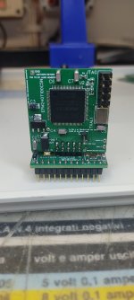
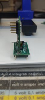
In case you are thinking of a nos/os system, I could make my latest Saa7220 pin compatible work available to the community. It features CPLD technology with code written by @miro1360 .I have these Chinese CPLD boards, so yes, I expect to use simultaneous mode. Not because it's magic (correct input signal conditioning is the "magic") buit to get 384kHz capability.
Thor
Attachments
-
 IMG_20240809_135829.jpg217 KB · Views: 87
 -
 IMG_20240809_135836.jpg163.9 KB · Views: 83
 -
 IMG_20240731_194531.jpg174.7 KB · Views: 90
 -
 IMG_20240731_194513.jpg210 KB · Views: 87
 -
 IMG_20240731_194525.jpg160.2 KB · Views: 80
 -
 IMG_20240731_193740.jpg131.8 KB · Views: 73
 -
 IMG_20240730_210441.jpg233.4 KB · Views: 83
- Home
- Source & Line
- Digital Line Level
- Building the ultimate NOS DAC using TDA1541A