Thanks for the great insight. CheersAnd Again - Decoding TDA1541 Power and Ground Pin's, the definitive edition
There is no spoon....
Please don't throw a metal spoon on the pcb

I think we have a name to that project : TDA1541A RPE (Red Pill Edition) 😎
TISNP is too difficult to pronounce while gently cool stupid for a pcb name 🙂
Perhaps No-Spoonization PCB ? .... Or Trinity for the three rails ??
Okay, I open a second bottle....
Please don't throw a metal spoon on the pcb
I think we have a name to that project : TDA1541A RPE (Red Pill Edition) 😎
TISNP is too difficult to pronounce while gently cool stupid for a pcb name 🙂
Perhaps No-Spoonization PCB ? .... Or Trinity for the three rails ??
Okay, I open a second bottle....

I think we have a name to that project : TDA1541A RPE (Red Pill Edition) 😎
I prefer TDA1541 insurrection!
Perhaps No-Spoonization PCB ? .... Or Trinity for the three rails ??
More seriously, +5V should be one of two innermost planes around TDA1541, with -15V twinned with that.
DGND should layer on top of +5V and extend to the rest of the digital circuitry.
AGND should layer on top of -15V.
Another -15V layer is needed below the TDA1541, so we can return all DEM Filter Capacitors and all local decoupling there.
So a 6-8 layer PCB (or veroboard, kapton tape and copper tape).
Thor
Now a friend warned me, I entered Iout incorrectly 😵, so with a Riv of 470R, the output voltage would be 1.8Vp-p. THD remains the same on a load of 10 Kohm.
@ThorstenL ,
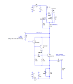
Not finding a third red wine of bottle, I went to the PCB CAD for a first concept draw of the close pcb around the tda1541A for the Insurection, Revolution, (I took already Extinction Deaf Rooster Edition for an ad1862 4 layers I have, so it is reserved) , Regurgitation, etc pcb !
To have a first idea of the close TDA1541A layout, I just worked here on 3 layers justto show the routing, each having a color; so it is not the layers layout but just to check the concept of conections and decoupling. The layout of the stargrounding to pin -15V (= new-AGND) seemed the shortest that way and maybe effective in spite of a plain ground for the real layout with the plain layer around the tda chip; at least a ground grille just below the chip and plain outside for the -15v could be perhaps only below the tda chips an idea also in spite of to proceed a plainer ground ?
The green is the the -5V pin, so new-DGND
the old-5V pin is not clear to me about his new Existenz ! but it is the new-DGND with no current outputting there so can be tied safely to the digital streaming front end (uf-l, clock, etc)
I have certainly made errors...
Because the 0.3V max compliance between the "grounds" in the datasheet, could it be safer to piggy back two diodes in opposite direction between the old-pin -5V/New-DGND and the old-15V/New-AGND somewhere far near the PS for instance ?
Edit, something is worrying me, how to connect pin 26 to 28 or their new avatars in order to programm the chip in simultaneous mode ?
Of course the red traces labelled -15V are the new AGND, i'm lazy so I didn't renamed the pin.
Attachments
Last edited:
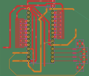
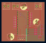
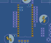
So it is just above to check the connections to see if I understood well Thorsten ! A6 to 8 layers will be of course with plain entire layers and no traces but the ones of the digital i2s front end, the reds you see till the uf-l pads for simultaneous mode.
Btw I have also drawned a core pcb economical 4 layers for working workshop purpose which is the real translation of the ugly conceptual safe check picture shematic of the post above, I have just to finish the DEM Grunding Lr connection to PIN 16/17. You got the idea : the green layer you can not see is the second layer :AGND (as the first red layer as well for the 14 DEMs: AGND both tied to pin 15) ;the green layer is layer in order to decouple the two audio current outputs; and in order to as well these two output traces do not see the DGND layer: the color brown dark you see below the i2s lines (it is now connected to the former -5V pin labelled now DGND); the last layer number 4 is the poluted +5Vconnected to pin 28 (which is both a power supply and a decoupling layer (the smd caps are on that layer at thebottom of the pcb).
It is easy to correct if I made errors. So to be clearer the post above 9030 :: The illustration represents a circuit schematic and is not intended as a PCB layout. It is just to show the decoupling and concept of where the return currents flows or should flow in a real layout.
that one below is a (simplified layout) real layout on 4 layers only but easy to make 6 (2 layers more to remove the -5V & +15V power traces).
Attachments
Last edited:
Wow clever boy Iggy. Me trying to digest & understand Thors post but too busy with work to think deep & clear. KudosSo it is just above to check the connections to see if I understood well Thorsten ! A6 to 8 layers will be of course with plain entire layers and no traces but the ones of the digital i2s front end, the reds you see till the uf-l pads for simultaneous mode.
Btw I have also drawned a core pcb economical 4 layers for working workshop purpose which is the real translation of the ugly conceptual safe check picture shematic of the post above, I have just to finish the DEM Grunding Lr connection to PIN 16/17. You got the idea : the green layer you can not see is the second layer :AGND (as the first red layer as well for the 14 DEMs: AGND both tied to pin 15) ;the green layer is layer in order to decouple the two audio current outputs; and in order to as well these two output traces do not see the DGND layer: the color brown dark you see below the i2s lines (it is now connected to the former -5V pin labelled now DGND); the last layer number 4 is the poluted +5Vconnected to pin 28 (which is both a power supply and a decoupling layer (the smd caps are on that layer at thebottom of the pcb).
It is easy to correct if I made errors. So to be clearer the post above 9030 :: The illustration represents a circuit schematic and is not intended as a PCB layout. It is just to show the decoupling and concept of where the return currents flows or should flow in a real layout.
that one below is a (simplified layout) real layout on 4 layers only but easy to make 6 (2 layers more to remove the -5V & +15V power traces).
Last edited:
So it is just above to check the connections to see if I understood well Thorsten !
If we do this, let's do it right.
We partially ignore what I will do, because of parts I have in stock.
Let's start with RF decoupling. We have the following pin's:
01 - LE - no decoupling
02 - BCK - no decoupling
03 - DAL - no decoupling
04 - DAR - no decoupling
05 - AGND - 0.47uF/1206 to VEE1 (GRM31C5C1E474JE1L)
06 - AOR - 0.01uF/1206 to VEE1 (GRM3195C1E103JA1D)
07 - DEM LSB - 0.047uF/1206 to VEE1 (GCM31M5C1H473JA6L)
08 - DEM BIT6 - 0.047uF/1206 to VEE1 (GCM31M5C1H473JA6L)
09 - DEM BIT5 - 0.047uF/1206 to VEE1 (GCM31M5C1H473JA6L)
10 - DEM BIT4 - 0.1uF/1206 to VEE1 (GCM31C5C1H104JA16K)
11 - DEM BIT3 - 0.22uF/1206 to VEE1 (GRM31C5C1H224JE2L)
12 - DEM BIT2 - 0.47uF/1206 to VEE1 (GRM31C5C1E474JE1L)
13 - DEM MSB - 2 X 0.47uF/1206 to VEE1 (GRM31C5C1E474JE1L)
14 - DGND - 0.47uF/1206 to VCC (GRM31C5C1E474JE1L)
15 - VEE1 (-15V) - 0.47uF/1206 to AGND (GRM31C5C1E474JE1L)
16 - DEM OSC1 - 1nF to 330R to 1nF to DEM OSC2
17 - DEM OSC2 - 1nF to 330R to 1nF to DEM OSC1
18 - DEM MSB - 2 X 0.47uF/1206 to VEE1 (GRM31C5C1E474JE1L)
19 - DEM BIT2 - 0.47uF/1206 to VEE1 (GRM31C5C1E474JE1L)
20 - DEM BIT3 - 0.22uF/1206 to VEE1 (GRM31C5C1H224JE2L)
21 - DEM BIT4 - 0.1uF/1206 to VEE1 (GCM31C5C1H104JA16K)
22 - DEM BIT5 - 0.047uF/1206 to VEE1 (GCM31M5C1H473JA6L)
23 - DEM BIT6 - 0.047uF/1206 to VEE1 (GCM31M5C1H473JA6L)
24 - DEM LSB - 0.047uF/1206 to VEE1 (GCM31M5C1H473JA6L)
25 - AOL - 0.01uF/1206 to VEE1 (GRM3195C1E103JA1D)
26 - VEE2 (-5V) - 0.47uF/1206 to VEE1 (GRM31C5C1E474JE1L)
27 - FMT - link to VEE2
28 - VCC (+5V) - 4 X 0.47uF/1206 to VEE1 (GRM31C5C1E474JE1L)
- 0.47uF/1206 to DGND (GRM31C5C1E474JE1L)
This means most pin's have a capacitor present.
The capacitors listed as decoupling are C0G dielectric, which is extremely high quality and generally superior to most film dielectric's and, offer the following decoupling performance:
Minimum impedance 7mOhm at ~7MHz and < 100mOhm 3MHz to 36MHz, with 300kHz - 380MHz below 1 Ohm.
These are the main decoupling capacitors for power supplies and MSB's, which I think a single capacitor is adequate.
All these capacitors listed belong below the TDA1541 or as close by as possible.
For a 4-Layer PCB I recommend the following, covering the area UNDER THA TDA1541 ONLY:
Single FR4 core
Inner planes DGND and AGND
Top plane +5V
Bottom plane 1 -15V extending to pin 26 only
Bottom plane 2 +5V at pin 27/28
We then place all decoupling capacitors below the PCB, next to each pin "pointing inwards".
As the DEM MSB pin's get 2 capacitors, these must be stacked on top of each other.
The 4pcs 0.47uF are also placed at the bottom between the +5V and -15V planes across the split between the planes at pin 27.
The capacitors at pin 14/28 are connected directly to the pin and using triple via's to the respective top layer planes.
We then need additional decoupling between the following pin's:
Pin 28 > Pin 15 - This is audio, RF should be handled by the RF decoupling below the TDA1541.
So perhaps Elna Silmic (if you are stocked up, as these are discontinued), or Nichicon Muse KZ, or film, e.g. WIMA MKS4B054706F00KSSD, 2pcs in parallel between pins 28 & 15. The WIMA film types listed will give a 200kHz minimum impedance of 1mOhm and < 0.1 Ohm to ~ 2MHz.
The impedance of our power supply needs considering, if we use a TL431 & boost transistor passing ~ 100mA we get 15mOhm per regulator, if we have three of these in series, this is 45mOhm so with 94uF the film capacitors are effective only above ~38kHz and the compound 431 being starts becoming inductive around 40kHz.
If we use TL431 directly, the impedance rises to ~0.45Ohm, the handover to the film capacitors drops to around 3.8khz and the point where the PSU becomes inductive rises to ~ 100kHz.
The most simple (and perfectly workable) PSU uses TL431 (TO-92 with TO-92 heatsink or SOIC-8 in SMT) without boost transistors and LM317 CCS in the negative lead (~100mA - 12 Ohm resistor) and a LM317 set to 27V with a 12 Ohm series resistor from it's output and a capacitor from the ADJ Pin (AC current source & DC regulator).
Other power supply options need to be considered too. If using Supercapacitors (e.g. Vishay/BC MAL222050007E3 25F/2.7V/26mOhm) this must be considered.
Pin 26 > Pin 15 - This is a Bias / CCS supply, use Panasonic Os-Con 1,000uF/16V (16SEPF1000M), 2pcs, minimum impedance 6mOhm @ 100...300kHz
Pin 28 > Pin 14 - This is a Digital CML supply, use Panasonic Os-Con 1,000uF/16V (16SEPF1000M), 2pcs, minimum impedance 6mOhm @ 100...300kHz
A low DCR choke (<= 1R) between DGND and AGND should be provisioned and tested. This should be placed at the PSU "0V" star.
Run Fat traces for the power supplies, deal with DGND and AGND at least as separate traces, if not adding a ferrite bead or choke to decouple the -5V ECL supply (aka DGND).
The protection diodes (back to back 1N5711) on AOL, AOR to AGND and between DGND & AGND should be added as well close to the IC.
Now, we extend the DGND ground plane outwards from the TDA1541 towards the digital circuitry.
I think enough work to draw schematics out.
But just BTB, we will use ECL if I have anything to say as relocking and part of signal conditioning, so MC10EL31DR2G as reclocker on LE (1pc) and MC10EPT20 as level translator on MCK, LE, BCK, DATAL and DATAR (5pcs) ...
Thor
Last edited:
I should add a few things to above missive.
The above assumed 4 X WCK for the DEM clock, on the principle to have the lowest practical frequency for DEM but to operate DEM mostly as intended.
Capacitors are sized for this (176.4kHz
No "grundig DEM reclock" please. This adds too much noise.
Use MC10EL31DR2G as final element in a divider chain from BCK. Feed MCK to the Clock pins via a level translator. Use 150R resistor to ground from each output.
We now have a differential clock with an ~ 1.6V P-P signal centered around 2V DC.
Use Tubee's circuit, that is 1nF on each OSC Pin (16/17) and a 330R resistor between them. Then one resistor each to the differential clock signal, forming an "L-Pad" with the 330R resistor. Precise value should be determined empirically to ensure that oscillator remains locked to our sync clock and has a stable output.
At a first guess, two more 470R resistors give ~0.4V P-P across 330R, when oscillating freely, we also see ~0.4V signal, Note that all this is strictly for our ECL driver as described above.
With DEM and LE relocked using ECL, the reclockers add no appreciable jitter. Bitclock and data probably do not or benefit from reclocking, but adding extra ECL flip-flops and relocking them will not do harm.
With MCK based on decent crystal oscillators, any jitter will be well below 100pS.
Thor
Hi Thorsten,
thanks, I just do this little core for you or Zoran if you want just for conveniance to use different circuitries at the front end, PS, and I/V in order to make life easier and have a cheap pcb tool proto to experiment faster. That's why I limited it to 4 layers to reduce the printing cost.
And also for the POC if one has a TDA1541A R grade to risk for the go/no-go.
Of course it is not the 6 or 8 alayers s I am an non tech enthusiast only with limited knowledge about layouting. This simple one took me a nigth, a complete one certainly several days. It is just to epress my gratitude and hapyness towards the you and the clever guys of the thread here that bring a lot to the comunauty.
But yes I agree on the philosophy: whatever pcb or DIY verroboard/copper and mylar tape, at the end it has to be made in order it measures good and sounds fine ! As you see I used just a CAD in the first picture as if it was a shematic, because for me it was just simplier to show and to ask like that in spite of a LT Spice shematic to know if my understanding was okay or not.
I should not have time the next days to correct it. But I follow the thread of course.
Thanks again Thorsten,
Last edited:
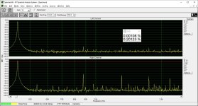
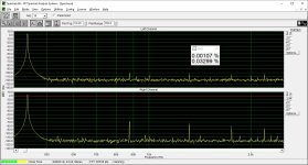
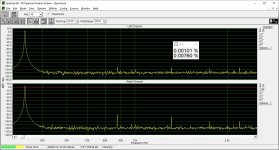
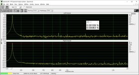
As promised. I/V resistors: 0, 2.2, 4.7, 10, 15, 22, 27, 33, 39, 47, 56, 68, 82 ohms. Distortion rises above 33 ohms. Top trace: Left channel (reference), bottom trace: Right channel (I/V resistor varied).
Attachments
-
 82_ohm.jpg154.2 KB · Views: 95
 -
 68_ohm.jpg150.5 KB · Views: 99
 -
 56_ohm.jpg147.9 KB · Views: 98
 -
 47_ohm.jpg147.2 KB · Views: 87
 -
 39_ohm.jpg146.7 KB · Views: 95
 -
 33_ohm.jpg146.5 KB · Views: 101
 -
 27_ohm.jpg146.1 KB · Views: 87
 -
 22_ohm.jpg147.4 KB · Views: 86
 -
 10_ohm.jpg145.8 KB · Views: 97
 -
 15_ohm.jpg145.6 KB · Views: 83
 -
 4-7_ohm.jpg146.5 KB · Views: 88
 -
 2-2_ohm.jpg146.6 KB · Views: 90
 -
 0_ohm.jpg148.4 KB · Views: 80
And with 2 mA offset compensation (Rout 2.5 k to +5 V), Riv = 68 ohms. THD is about the same as 33 ohms without offset compensation, as expected.
Offset current compensation has the additional advantage that no output coupling capacitor needed, if the I/V converter is the data sheet operational amplifier topology.
Offset current compensation has the additional advantage that no output coupling capacitor needed, if the I/V converter is the data sheet operational amplifier topology.
Attachments

As promised. I/V resistors: 0, 2.2, 4.7, 10, 15, 22, 27, 33, 39, 47, 56, 68, 82 ohms. Distortion rises above 33 ohms. Top trace: Left channel (reference), bottom trace: Right channel (I/V resistor varied).
This is very interesting.
I find it a little different to understand what we see?
A 0dBFS signal at 450Hz?
What is the "reference" circuit and what is the circuit where the I/U conversion resistor is varied (without apparently varying the levels)?
It is probably worthwhile to also consider the data here:
https://www.mvaudiolabs.com/digital/tda1541-iv-resistor-selection/
I find it interesting that while up to ~30...35 Ohm are ok and have low distortion, we see improvements (especially lower high order components once we go below 5 Ohm. Sadly your test cuts of at H4 so we cannot evaluate H5 - H10.
Overall your tests do however show similar results as on MVAL. Thank you for all the hard work and confirming existing data independently.
Thor
@lcsaszar , thanks for the very useful datas 🙂
.
Maybe the 2mA current should be point to -15V? As pure amalog?
I dont know?
.
In that light these reference currents at the pictures, marked as "ground", from CCS comparsion
IN real circuit. Not that one suplying the circuit with constant current. For the example, last one with JFET does not have any "outside" tap reference...
I thinj that (R5, R10 1st), (R4 2nd), (R2 3rd) should be connected, with multilied values, to -15V point
.
Maybe the 2mA current should be point to -15V? As pure amalog?
I dont know?
.
In that light these reference currents at the pictures, marked as "ground", from CCS comparsion
IN real circuit. Not that one suplying the circuit with constant current. For the example, last one with JFET does not have any "outside" tap reference...
I thinj that (R5, R10 1st), (R4 2nd), (R2 3rd) should be connected, with multilied values, to -15V point
- Home
- Source & Line
- Digital Line Level
- Building the ultimate NOS DAC using TDA1541A