btw the IV stage is really challenging
since there are no one confirmed yet
which one is the best IV converter for TDA1541 dac
If I had to use a I/V converter for a TDA1541A DAC right now, I would choose passive I/V conversion (resistor for converting a current into a corresponding voltage).
But there is one problem, TDA1541A +25mV and -25mV output compliance. The more this output compliance is exceeded, the higher the distortion. The limit for the I/V resistor is around 68 Ohms (good trade off between slightly increased distortion and reasonable output signal amplitude)
This results in 0.004 (full scale output current in A) * 68 Ohms = 272mVpp output voltage.
Without further corrections the TDA1541A output signal then swings between 0V and -272mV, exceeding -25mV output compliance by -247mV.
Why is this? TDA1541A idle current equals -0.002mA and the current swings between 0mA and -4mA, so the current never gets positive.
If we can obtain symmetrical swing around 0V DC, output compliance would only be violated by -136mV and +136mV instead of 0mV and -272mV.
Symmetrical swing (0 volts DC on the TDA1541A output) can be obtained by:
- Injection of +2mA bias current for each TDA1541A output. Problem here is unavoidable DC drift and CCS impedance varying with frequency. I tested +200V high voltage supply with 100K current limiting resistor for CCS replacement, it works excellent but the high voltage is dangerous to work with.
- Placing a small DC voltage between GND and the I/V resistor, nulling the DC voltage on the TDA1541A output.
I personally prefer the DC compensation voltage method as it is very stable (no drift), easy to implement and only requires a safe low supply voltage of +15V.
Suppose we use a 68 Ohm I/V resistor and the DC voltage we need to add is 0.002 (TDA1541A idle output current) * 68 = 136mV.
Suppose we have a +15V DC voltage available (7815 or improved voltage regulator for example)
Then we could place 6.8 Ohm resistor between 68 Ohm and GND like this:
TDA1541A output (signal output) -> 68 Ohms (junction) -> 6.8 Ohms -> GND
In order to null the DC on the TDA1541A output we need approx. (15 - 0.136) / 0.02 = 743.2 Ohm resistor between junction and +15V. We can use 680 Ohms in series with a 250 Ohm multi turn trimmer for fine adjustment (0V DC on the TDA1541A output).
Because there is no DC on the TDA1541A output (DC-coupled) and we get 272mVpp signal swing, this signal can be directly fed into a standard pre amplifier.
This means the entire I/V converter consists of a 68 Ohm resistor, 6.8 Ohm resistor, 680 Ohm resistor, 250 Ohm multi-turn trimmer and a +15V regulator.
hello John,
glad to have an answer from the expert here, thanks

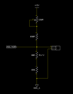
btw i try to figure out into a simple schematic what i can understand from your explanation, is this correct?
and is it compatible with TDA1541 non-A ??
thanks.
Attachments
btw i try to figure out into a simple schematic what i can understand from your explanation, is this correct?
and is it compatible with TDA1541 non-A ??
Almost correct, I attached the corrected version. Yes this also works for the TDA1541 non A version.
Attachments
not sure which one would be the best but most of them won't work without nulling -2mA offset coming from TDA1541A, unless TDA1541 is different than TDA1541A in that matter.
I am very happy with my current DAC, but I would like to build TDA1541A DAC in simultaneous mode, with Ian I2S to PCM, isolators, FIFO buffer (I purchased back in 2015), ultra-low output impedance shunt regulators (from Salas), Pedja Rogic approach to decoupling and I/V conversion. Being lazy... is there any information on how Ian did his TDA1541A dac? what is the chain of the modules etc? Thanks in advance.
hi Ripson,
what DAC you are using now?
for now i'm only focusing for the IV stage
not yet for the converter or isolator or fifo etc...
besides its too complicated for me😕
maybe later i2s to simultaneous to play with🙂
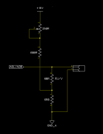
Almost correct, I attached the corrected version. Yes this also works for the TDA1541 non A version.
oh, i see
thank you for the correction John
should we add a smoothing capacitor here?
maybe a caps parallel with the R.iv or trimmer?
regards
what do you purpose for voltage amplification with passive I/V?
I think it's for nulling DC on the TDA1541A output (DC-coupled) so the signal can be directly fed into a standard pre amplifier.🙂
oh, i see
thank you for the correction John
should we add a smoothing capacitor here?
maybe a caps parallel with the R.iv or trimmer?
regards
and also which resistor should have a bigger watt?
the 68R or 6R8 ??
thanks.
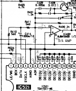
Sony was using a similar scheme back in the time of CDP-950 - they had the design flaw of only providing +5V to the opamps. But they where using quite large capacitors in that current offset path (see attached snapshot of the schematic). stupid Sony style of schematics though...
Attachments
Sorta of active voltage loaded I/V with the R in the feedback loop of the oap ? 🙁 measure fine but sounds 😱 ?
Is that so different sonically than a good CCS for the output compliance with non feedbacked BJT neutral diamond style active stage after that is happy with the high output impedance of the TDA1541A ?
Is that so different sonically than a good CCS for the output compliance with non feedbacked BJT neutral diamond style active stage after that is happy with the high output impedance of the TDA1541A ?
I can't comment on the I/V converters you collected, because I never tried them, but this one that I built and tested:which one of these iv are best for tda1541??
https://www.diyaudio.com/community/attachments/dac_tubeout-1-jpg.1002809/
This is different from the others in the input mode: it accepts differential input from a single DAC (one TDA1541A provides L+ and L-, another TDA1541A provides R+ and R-). Simple way of creating an analog push-pull signal in the digital domain is to feed an inverted DATA stream to the L- or R- digital input. Although it causes a theoretical 1-bit offset, it is unnoticable. Marantz uses this trick in CD-94 Mk II.
I found an I/V transformer effectively filters unwanted aliasing images beyond the audible frequency range.
I can't comment on the I/V converters you collected, because I never tried them, but this one that I built and tested:
The circuit is interesting, I already noticed it quite some time ago. But it contains a number of imperfect components that are going to degrade the signal one way or the other.
Every tube (even same type brand and batch) sounds different and keeps changing as the tube burns in and ages.
Every transformer (same transformation ratio, same power rating) sounds different. This is also true for output and inter-stage transformers in tube amplifiers. The most expensive one's often perform best, so good performance usually comes at a high price.
Same with coupling caps, I tried -many- including V-cap TFTF, Duelund copper foil and so on, and again, every coupling cap sounds different and performance keeps changing as the materials (plastic, resin, foil) settle. Again, the best performing (most neutral sounding) capacitors come at a high price. The application also matters, so we need specific caps for use in tube circuits where high DC voltages are likely to appear across the caps.
Tubes have their charm and seem to be more "compatible" with music compared to semiconductors. It is fascinating to fiddle around with imperfect components causing all kind of interesting problems.
Transformers won't filter aliasing images, this requires (digital) filters with "brick wall" characteristics, but step up transformers with limited bandwidth will attenuate unwanted RF signals.
Anyway, analogue circuits are -always- lossy and unstable (thermal drift). So why keep using these lossy solutions (including lossy amplifiers) when we have the luxury of a digital audio source?
I mostly agree. A true digital power amplifier, and a true digital loudspeaker with 65535 individually activated unity-pressure tranducer elements would be best.
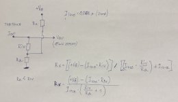
Hi EC 🙂In order to null the DC on the TDA1541A output we need approx. (15 - 0.136) / 0.02 = 743.2 Ohm resistor between junction and +15V. We can use 680 Ohms in series with a 250 Ohm multi turn trimmer for fine adjustment (0V DC on the TDA1541A output).
I just spot that maybe a slight mistake occured?
Probably should be: (15V - 0.136V) / 0.002A = 7432ohms. then 6800ohm + 1K pot set to 7432-6800=632ohms
?
cheers
Last edited:
I made a mistake too 🙁
But I checked, and this is right formula to calc values:
.
for Vb=+15V, Iidle=0.002A Riv=68ohm and Ra=6.8ohm Rx=675.6ohm
.
(Note, that in this case, from Rx to Ra, will be 22mA,
Rx could be made from 620ohm and 100ohm multiturn pot set to 55.6ohm, or 0mV offset)
But I checked, and this is right formula to calc values:
.
for Vb=+15V, Iidle=0.002A Riv=68ohm and Ra=6.8ohm Rx=675.6ohm
.
(Note, that in this case, from Rx to Ra, will be 22mA,
Rx could be made from 620ohm and 100ohm multiturn pot set to 55.6ohm, or 0mV offset)
Attachments
Last edited:
Just out of curiousity, what is wrong with a maybe simple style current injection like this?
Used 5v on pic but +15 can be used here too just 7.5k resistor instead of 2.5k

(I can see if using +5v of vdd from dac (for convenience) you would also inject noise into output, while fresh +15 with no other loads would be cleaner)
P.S i still feel bad havent gotten around to replying to your troubleshooting help, but have not forgotten about it.
Need 2-3 days in a row free to take whole dac apart, change voltages on regulators, mess with everything etc...
Best regards
Edit: i like this new forum front end, you can just screenshot (win+shift+S) and ctrl+v image straight into post..
Used 5v on pic but +15 can be used here too just 7.5k resistor instead of 2.5k
(I can see if using +5v of vdd from dac (for convenience) you would also inject noise into output, while fresh +15 with no other loads would be cleaner)
P.S i still feel bad havent gotten around to replying to your troubleshooting help, but have not forgotten about it.
Need 2-3 days in a row free to take whole dac apart, change voltages on regulators, mess with everything etc...
Best regards
Edit: i like this new forum front end, you can just screenshot (win+shift+S) and ctrl+v image straight into post..
I think nothing? You can choose one of several ways proposed for current injection?
.
(Bare in mind that current should be out of the phase in Your circuit. At Riv voltage is in phase, first going into the +region, but should be out-of-phase and firs to go into negative V region...
To verifiy this, try to simulate classic OPamp design and 0deg phase and You will see right current source polarity, and in-phase voltage output. 🙂
But anyway, this small voltage should be amplified to some line level, and single stage, single ended amplification, (JFET, Tube, BJT) shifing the phase back to 0deg.
And add serial resistor of about 1800ohms after the current source. That is about output resistance of the dac i think?)
.
cheers
.
(Bare in mind that current should be out of the phase in Your circuit. At Riv voltage is in phase, first going into the +region, but should be out-of-phase and firs to go into negative V region...
To verifiy this, try to simulate classic OPamp design and 0deg phase and You will see right current source polarity, and in-phase voltage output. 🙂
But anyway, this small voltage should be amplified to some line level, and single stage, single ended amplification, (JFET, Tube, BJT) shifing the phase back to 0deg.
And add serial resistor of about 1800ohms after the current source. That is about output resistance of the dac i think?)
.
cheers
Last edited:
Hi EC 🙂
I just spot that maybe a slight mistake occured?
Probably should be: (15V - 0.136V) / 0.002A = 7432ohms. then 6800ohm + 1K pot set to 7432-6800=632ohms
The voltage across 6R8 = +0.136V
So the current running through that resistor must be I = V / R = 0.136 / 6.8 = 20mA or 0.02A.
So the calculated values are correct. Note that this is a bias voltage correction (lifts up the I/V resistor ground potential) rather than a bias current correction. So the bias current through the voltage divider can be much higher (20mA in this case) than the actual TDA1541A idle current of 0.002A.
Just out of curiousity, what is wrong with a maybe simple style current injection like this?
Used 5v on pic but +15 can be used here too just 7.5k resistor instead of 2.5k
View attachment 1004615
(I can see if using +5v of vdd from dac (for convenience) you would also inject noise into output, while fresh +15 with no other loads would be cleaner)
P.S i still feel bad havent gotten around to replying to your troubleshooting help, but have not forgotten about it.
Need 2-3 days in a row free to take whole dac apart, change voltages on regulators, mess with everything etc...
Best regards
Edit: i like this new forum front end, you can just screenshot (win+shift+S) and ctrl+v image straight into post..
Just out of curiosity, what is wrong with a maybe simple style current injection like this?
Used 5v on pic but +15 can be used here too just 7.5k resistor instead of 2.5k
Yes this will work too, but you get power supply noise injection that can only be reduced by increasing the series resistor value and supply voltage. This is the solution with +200V supply and 100K series resistor I mentioned. This was the best performing circuit I tested with bias current injection.. It offers approx. 1470 times supply noise/ripple attenuation. It also creates a more ideal constant current source.
With the reference voltage that lifts up the I/V resistor ground potential, we can easily bypass the 6R8 resistor with say a 10000uF/6.3V capacitor. This way we can greatly reduce power supply noise injection compared to the series resistor solution and don't need high supply voltages.
I mostly agree. A true digital power amplifier, and a true digital loudspeaker with 65535 individually activated unity-pressure tranducer elements would be best.
Here is my personal final solution for the ultimate NOS DAC, a quest that was started in 2006.
My idea is removing -all- (digital) amplifiers and active analogue circuits from the signal path. It is difficult to grasp the idea of driving a speaker without -any- amplifier.
The goal is maintaining the lossless digital signal path all the way up to the speaker, eliminating the complete conventional analogue signal path including all related distortion and degrading.
I ended up with this:
Digital audio data (numbers) -> digital switch combinations -> precision power resistor array -> speaker. The device received the name PowerDAC-S.
It is basically a programmable resistive attenuator, suitable for directly driving speakers. Its is designed such way that its output impedance is constant.
One -could- view it as an ultra high speed stepped attenuator connected to a power supply where the speaker connects to the attenuator output. This way we can generate analogue signals without the need for analogue circuits like (pre) amps.
It is easy to come up with a theory, but it is very difficult to translate a theory into a practical working circuit. We also had to fix the well known digital audio receiver problems like jitter & noise spectrum.
I attached the PowerDAC-S block diagram.
On the left we have the S/PDIF DAPI (Digital Audio Parallel Interface) receiver. It basically receives a S/PDIF stream and outputs left and right channel parallel data accompanied with one single sample clock signal:
Parallel data left, Parallel data right, sample clock (44.1 KHz ... 192 KHz).
Because we no longer generate nor use I2S or comparable serial digital audio interfaces, related high frequency clocks and serial data signals are no longer present here.
The parallel data enters two Fractal decoders, these basically chop up the highest and most critical bits into 31 fragments that represent said higher bits. So the data (numbers) remain the same, but are simply represented differently. So instead of 256 for example we express the number as 64 + 64 + 64 + 64, same result, smaller numbers. At this point we still have a digital (lossless) signal.
So why on earth do we chop up the higher bits? by doing so we can minimise bit errors with given high output current and given switch limitations (RDSon). We can minimise glitches and we can easily achieve required low output impedance. Finally we can use standard SMD thin film precision power resistors as the total power is now divided over 31 smaller resistors. The resistors are thermally coupled to a large heat sink.
Parallel 44 bit data for L and R channels enter parallel latches that provide sample timing (sample clock). All outputs now change at exactly the same moment. The signal is still lossless (digital).
The latches drive ultra high speed bit switches. The switch outputs are still digital (lossless).
So up to this point we are still dealing with exactly the same numbers (sample values) as stored in the digital audio file, there are no losses that would typically occur with analogue circuits and we are already very close to the output (speaker).
The switches drive a thin film precision power resistor array and here the still lossless digital signal is converted to analogue. But resistors are pretty linear and offer huge bandwidth (SMD components, low inductance, low capacitance), so losses are very limited compared to active analogue circuits that are always based on non-linear components.
Converter efficiency is low, 12.5% max, measured efficiency equals 10.8%. Efficiency is further reduced by the programmable linear power supplies. So for say 2 x 4W output power we need to dissipate approx. 120 watts continuous. Therefore the practical output power is limited and we have to use suitable speakers with reasonable sensitivity in order to get jack hammer SPL with only 2 x 4W converter output.
The remaining problem is volume control, the conventional analogue signal path no longer exists with the PowerDAC-S, so how do we control the volume?
Volume is controlled by a combination of supply voltage programming (higher supply voltage, higher volume, higher power dissipation in the resistor array) and bit alignment or bit shifting. The power supply voltage sets the "gain" and the bit shifts set the digital attenuation. By combining both we get a lossless (no audible degrading) volume control over a practical range (remember, no more amplifiers, no more gain / attenuation matching required).
The PowerDAC-S cannot clip as the speaker input = DAC output. The PowerDAC-S can drive any load between dead short and infinity. There are no local or global feedback loops at all, so the circuit is always fully stable and cannot oscillate. Bandwidth limitation that is always required with (pre) amplifiers in order to guarantee stable feedback operation is no longer required here. We theoretically have 200 MHz bandwidth with the PowerDAC-S, this bandwidth is obviously reduced by (speaker) wiring and parasitics.
Toslink is well known for related jitter issues, this is usually caused by the S/PDIF receiver that recovers the source clock and fails to block contained jitter. The PowerDAC-S is based on a S/PDIF DAPI receiver that extracts only the data from the incoming stream and places this data in a data buffer. This data is then output in parallel, accompanied with an independent, clean sample timing signal that is directly derived from a local, low phase noise master clock. The source noise problem is tackled by the Toslink interface (perfect galvanic insulation, limited bandwidth) and DAPI.
I also attached some pictures of the PowerDAC-S during the final development stage. So this is not just a theory, the practical circuit is up and running and 4 of these have already been built, for me personally there is no way back to analogue circuits as I am very spoiled now.
Attachments


Hi Yes I corrected the statement in next post sorry 🙂 https://www.diyaudio.com/community/...ate-nos-dac-using-tda1541a.79452/post-6876813The voltage across 6R8 = +0.136V
So the current running through that resistor must be I = V / R = 0.136 / 6.8 = 20mA or 0.02A.
So the calculated values are correct. Note that this is a bias voltage correction (lifts up the I/V resistor ground potential) rather than a bias current correction. So the bias current through the voltage divider can be much higher (20mA in this case) than the actual TDA1541A idle current of 0.002A.
and gave the more acurrate formula to calculate values of resistors acording to +V used.
Please see attachment
.
But is the re any proposed ratio with Riv and small value R from Riv to GND? In Your example that is 10/1...
Very interesting ecdesigns, thanks for sharing! Never seen something like this, elegant solution. Even the prototype seems tidy. Wonder how it sounds...
Btw since its built, may we inquire what is the thd+n?

Btw since its built, may we inquire what is the thd+n?
Good idea..injecting 0.1v p-p 100khz noise in the biasing supply, the parallel cap greatly attenuates. Thank you for sharing knowledge John and Zoran.With the reference voltage that lifts up the I/V resistor ground potential, we can easily bypass the 6R8 resistor with say a 10000uF/6.3V capacitor. This way we can greatly reduce power supply noise injection compared to the series resistor solution and don't need high supply voltages.
- Home
- Source & Line
- Digital Line Level
- Building the ultimate NOS DAC using TDA1541A