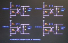
Audial AYA DAC USB simultaneous mode
Hi all:
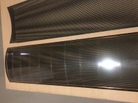
To refocus the debate on the topic I leave here a few pics about some of my latest attempts to improve (the already great) AYA DAC.
In my humble opinion what most improves the sound:
- Audial USB board in simultaneous mode;
- Vishay Z-Foil resistors;
- Audio Note copper foil capacitors;
- 1uf/50V Sanyo Os-con capacitors around TDA1541;
- 10uf/50V Elna Silmic II around I/V and buffer op-amps
- Allen Bradley 1W resistors after diodes.


I hope you enjoy it and that the authorities (like summotan) comment on this.
Long life to the TDA1541A!
Hi all:
To refocus the debate on the topic I leave here a few pics about some of my latest attempts to improve (the already great) AYA DAC.
In my humble opinion what most improves the sound:
- Audial USB board in simultaneous mode;
- Vishay Z-Foil resistors;
- Audio Note copper foil capacitors;
- 1uf/50V Sanyo Os-con capacitors around TDA1541;
- 10uf/50V Elna Silmic II around I/V and buffer op-amps
- Allen Bradley 1W resistors after diodes.
I hope you enjoy it and that the authorities (like summotan) comment on this.
Long life to the TDA1541A!

.. He immediately withdrew it and maturely apologized. And for some reason we are still hearing fallout from it. Time to close that 4 year old incident and move on.
It reads to me that this was only mentioned to provide some contextual truth. Also the term 'lip service' comes to mind; where someone says whatever they 'need' to say in order to direct the outcome in their favor - which loops back to the issue of morality.
So far as 'moving-on' - I'm sure that if the original offender kept his nose out of this thread (Rj - you have your own thread now) and without antagonistic posts which support the rise of slanderous comments such as likening someone to a shocked rat, strangely/naively coupled with support for the Rj false morality, then perhaps with time this might be possible.
As they say, treat the cause and not the reaction - in this instance treating the cause is easy; "Ryanj: stay at home".
Last edited:
Hi all:
To refocus the debate on the topic I leave here a few pics about some of my latest attempts to improve (the already great) AYA DAC.
In my humble opinion what most improves the sound:
- Audial USB board in simultaneous mode;
- Vishay Z-Foil resistors;
- Audio Note copper foil capacitors;
- 1uf/50V Sanyo Os-con capacitors around TDA1541;
- 10uf/50V Elna Silmic II around I/V and buffer op-amps
- Allen Bradley 1W resistors after diodes.
I hope you enjoy it and that the authorities (like summotan) comment on this.
Long life to the TDA1541A!
That all looks really good!.. have to say that I also have an older version of the same board and it plays just as you know it does; wonderfully well.
Hi all:
To refocus the debate on the topic I leave here a few pics about some of my latest attempts to improve (the already great) AYA DAC.
In my humble opinion what most improves the sound:
- Audial USB board in simultaneous mode;
- Vishay Z-Foil resistors;
- Audio Note copper foil capacitors;
- 1uf/50V Sanyo Os-con capacitors around TDA1541;
- 10uf/50V Elna Silmic II around I/V and buffer op-amps
- Allen Bradley 1W resistors after diodes.
View attachment 971162
Nice, did you perform a before & after sound test when you change the rectifier diodes & the AB carbon resistors, if so what's your findings ?
I suppose the AB's add warmth as your using naked foil resistors on i/v stage & after.
Thanks
View attachment 971163
I hope you enjoy it and that the authorities (like summotan) comment on this.
Long life to the TDA1541A!
Very interesting thread here, I was browsing through it but it's faily long so still trying to catch up to everything, please bear with me..
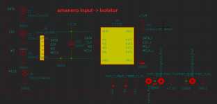
I'm thinking of making an usb input pcb with an isolator, i2s-sim and dac (for non-commercial usage, and i will post finished/tested gerbers here). 🙂
For this purpose, was wondering which schematic design is the latest, the one in post #6077? There's many different styles of DEM reclock at this point, not sure what is the best current practice in 2021. 50hz DEM?
Is post #6315 or #6079 i2s to simultaneous converter more recommended? I am leaning towards #6315. Maybe #7092 but i dont need balanced.
The chain i hope to work is USB amanero-> il715 isolation-> i2s to simultaneous-> DAC -> Rogić's diamond diff I/V (or lampizator srpp).
Will probably use Jung/Didden's superregs instead of lm78/79 for the power rails, but still include the provided regulation on the pcb's.
I believe post #6077 represents SOTA. 50Hz DEM. Also find signal attenuation circuits earlier in the thread. He also supplied some PS circuit suggestions. If you follow 6077 you'll do well.
I believe post #6077 represents SOTA. 50Hz DEM. Also find signal attenuation circuits earlier in the thread. He also supplied some PS circuit suggestions. If you follow 6077 you'll do well.
Thank you for the advice! I might but be wrong, but i thought we dont need attenuators with the converter because of the 2.5V VDD supply for the IC's, the output is then similarly lowered? But i guess it wouldn't hurt to throw something like #4336 right before it the sim converter. Maybe even before the isolator? I'm not sure..this is not my strong field
Don't wanna get involved and correct me if im wrong but...i noticed this too, copy paste of John's design selling for 15$/PCB and 150$ populated? They are not gold plated and who knows if its even 4 layer. In quantities of 50+ this is easily under 1$ per PCB (from JLC). Components is 10$ at most (even with MOQ's of 5 or more, so actually less per unit). No offense to him, because he is offering the convenience to people and his time to send them as well, those who dont like it don't have to buy but....For the story, after you close all the exchange in the public thread which was not made for you to grab all and make after your own board without credit and care to the community that helped you as you sold it since the beginning at more than x20 the price of JPLCB printing - [....]
This is a part of the reason why i decided to make my own board, and moreover publish everything you need to print them yourself here. If John and others have graciously provided their time and knowledge to the DIY community then it would be good to give the people wanting to build them more options.
regarding signal attenuation
Contrary to some of the recent chatter, Ryanj did quite a bit of research wrt attenuation with testing, measurement and listening tests using:
-no attenuation (his D1)
-and each of the two circuits suggested by John, aka ecdeisgns
He claims better sound with attenuation, and found one of the two proposed designs to be subjectively more satisfying. He also shared sound clips showing the difference between the two attenuation schemes. I recall even with a recorded clip it was clear.
For easy reference you can see the implementation of the preferred version of John's circuit in Ryan's final design. His circuit is openly shared here:
D3 Schematics.PDF - Google Drive
The project is documented here with full credit to all contributors.
https://www.diyaudio.com/forums/group-buys/328060-diy-tda1541a-pcb-d3.html#post5558101
Hope this makes the search through years of posts easier. 🙂
Brilliant, yes it does help the search greatly! Much appreciated Wlowes (and Ryan) 😀
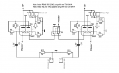
This is progressing swimmingly but the hardest part is still ahead, mixed signal PCB design. Im designing 3 other PCB's in parallel as well, and you can only do so much in a day so pointing out important posts i probably missed is of course appreciated 🙂
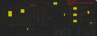
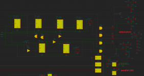
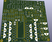
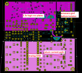
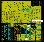
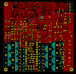
Finished the preliminary layout of the board, I would appreciate any input to see if i made any major blunders.
-4 layer board
-GNDA and GNDD is on different planes, but connected together at the source (afaik logic return currents should not touch the analog at all)
-3 different options of bypass caps, populate as you wish
-excesive number of headers, jumpers and u.fl's in case you want to bridge something, use external PSU's for everything, or bypass certain sections. For example you can keep the whole DIR9001 section off if your input is from amanero/xmos.
-i2s attenuation
-Il715 isolator on input
-plenty of stitching vias
That is it, you pretty much know the drill if you've been following the thread, thanks once again to John and others for their contributions!! 😀
The board is a bit tight because my absolute requirement was that it be 100x100mm or less, this is exactly 100x100mm.
I have posted images here on imgur album, and in the post itself.
Pictures album
I tried to write text on them to make it a bit easier to go through, and at the end are included screenshots of the schematic that this is based on. (on
I will wait for a couple of peer reviews, after that get the board fabricated, then test it, and then post the gerbers. Thank you!
Attachments


L0rdGwyn's posts on a PCM56 bases DAC have been moved here in order to maintain the purity of this thread.
If any more posts should be moved or you want a different title then please add the requests to the new thread and they will be done.
EDIT... the above 'thread split' is now deleted as a new thread may be forthcoming.
The game is up! I've been found out, it was a good run.
I certainly don't want to taint the purity of this thread - thank you for the early advice that was given here, I will continue my exploits elsewhere 🙂
I certainly don't want to taint the purity of this thread - thank you for the early advice that was given here, I will continue my exploits elsewhere 🙂
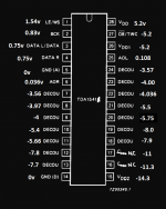
Built and assembled DAC in post #7972 (just above) but having bit of an issue..
Sound coming out is very distorted and crackling, almost like somebody blowing into the mic. Hard to tell even what music is playing really..
I am using Amanero as source and tried all bit depths and sampling rates, and bit depth doesn't change it much but 384khz sample rate improves it somewhat (but issue is still there).
When nothing is playing, there is a digital sounding "buzz" which im pretty sure is BCKO related.
Some voltages measured (also see on attached image):
LEO - 1.5v
BCKO - 0.83v
DOL&DOR - 0.755v
I am not sure what voltages it is expecting (maybe it is way too low)
so i thought maybe there is too much attenuation on I2S lines (i am using 33R from ecdesigns to limit slew rate but after that also the attentuation scheme from D3 dac (you can see schematic in post #7972), so i tried messing with it, bridging some resistors, and bypassing the whole i2s-sim thing by using the provided J9 header (next to up left corner on dac), but it sounds probably even worse.
Then i thought maybe it is because using non-A chip, and DEM reclock part is messing with it, but removing the 12k resistor makes no difference.
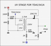
Maybe DAC chip is bad but it worked at the point when i gently removed it from a philips player (which is now torn down). Its not even heating very much, barely warmer than skin. Only decoupling caps installed are 100nF and 120uF for MSB. I/V is ecdesigns passive with 150R.
Anyway i attached a pic of voltages i measured on the DAC when nothing is playing. There is suspiciously more DC offset on AOL than AOR, and somehow some voltages are weird, example pin 12 voltage is lower than pin 13 (which i thought is MSB?).
Of course also checked for cold solders, bridges on the smd logic, but everything looks ok..
Would appreciate any help / thoughts..
Sound coming out is very distorted and crackling, almost like somebody blowing into the mic. Hard to tell even what music is playing really..
I am using Amanero as source and tried all bit depths and sampling rates, and bit depth doesn't change it much but 384khz sample rate improves it somewhat (but issue is still there).
When nothing is playing, there is a digital sounding "buzz" which im pretty sure is BCKO related.
Some voltages measured (also see on attached image):
LEO - 1.5v
BCKO - 0.83v
DOL&DOR - 0.755v
I am not sure what voltages it is expecting (maybe it is way too low)
so i thought maybe there is too much attenuation on I2S lines (i am using 33R from ecdesigns to limit slew rate but after that also the attentuation scheme from D3 dac (you can see schematic in post #7972), so i tried messing with it, bridging some resistors, and bypassing the whole i2s-sim thing by using the provided J9 header (next to up left corner on dac), but it sounds probably even worse.
Then i thought maybe it is because using non-A chip, and DEM reclock part is messing with it, but removing the 12k resistor makes no difference.
Maybe DAC chip is bad but it worked at the point when i gently removed it from a philips player (which is now torn down). Its not even heating very much, barely warmer than skin. Only decoupling caps installed are 100nF and 120uF for MSB. I/V is ecdesigns passive with 150R.
Anyway i attached a pic of voltages i measured on the DAC when nothing is playing. There is suspiciously more DC offset on AOL than AOR, and somehow some voltages are weird, example pin 12 voltage is lower than pin 13 (which i thought is MSB?).
Of course also checked for cold solders, bridges on the smd logic, but everything looks ok..
Would appreciate any help / thoughts..
Attachments
Hi Zbunjen,
In general it is best to build a breadboard setup and test circuits thoroughly before even thinking of routing a PCB.
I suggest to test sub systems to locate the problem.
First check if the TDA1541 (still) works correctly:
- Check all supply voltages and grounding
- Connect TDA1541 pin 27 to +5V (I2S time multiplex mode)
- Remove all I2S attenuators
- Feed I2S directly into the TDA1541
- Remove I/V converter circuit and connect 33 Ohms between analogue output and GND. Then route the signal to a suitable (pre) amplifier or headphones
This will require some pin lifting, interrupting PCB traces or temporarily remove parts.
If the TDA1541A works, connect the I2S attenuators and modify these if there are problems. The I2S attenuators are critical and because of given chip tolerances it may be necessary to re-adjust average DC level or increase peak to peak signal level for reliable operation.
If the problem is located in the glue logic (SIM decoder) you probably need an oscilloscope to check all related signals and verify these with datasheet specs.
I hope the mods don't get mad at me, but I finished my PCM56 DAC.
PCM56 DAC Build
I only post it here because this is the thread where I first asked questions on NOS R2R DAC design, so thank you for sending me on the right path, very happy with how it turned out 🙂 much appreciated.
PCM56 DAC Build
I only post it here because this is the thread where I first asked questions on NOS R2R DAC design, so thank you for sending me on the right path, very happy with how it turned out 🙂 much appreciated.
ohmy... this is almost 2022
and this vintage '80s dac still have a lot of fans today😀
including me...😉
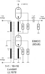
btw the IV stage is really challenging
since there are no one confirmed yet
which one is the best IV converter for TDA1541 dac
to be more concise
i collected some of them here,
which one of these iv are best for tda1541??
thanks.
Peter
and this vintage '80s dac still have a lot of fans today😀
including me...😉
btw the IV stage is really challenging
since there are no one confirmed yet
which one is the best IV converter for TDA1541 dac
to be more concise
i collected some of them here,
which one of these iv are best for tda1541??
thanks.
Peter
Attachments
-
 OUTPUT.jpg95.9 KB · Views: 333
 -
 TDA1541AIV.png50.5 KB · Views: 324
 -
 TDA1541_tubed_CCDA.jpg128.8 KB · Views: 404
 -
 dac_tubeout (1).jpg59.9 KB · Views: 564
 -
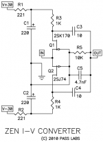 z_IV_3.png32.4 KB · Views: 345
 -
 red.png45.9 KB · Views: 295
 -
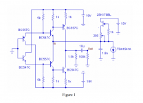 diamond.png45.7 KB · Views: 300
 -
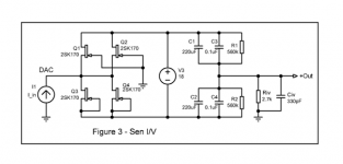 SEN.png22.7 KB · Views: 297
 -
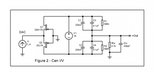 CEN.png19.4 KB · Views: 285
 -
 tube-i-zator.png131.4 KB · Views: 329
Last edited:
which one of these iv are best for tda1541??
not sure which one would be the best but most of them won't work without nulling -2mA offset coming from TDA1541A, unless TDA1541 is different than TDA1541A in that matter.
I am very happy with my current DAC, but I would like to build TDA1541A DAC in simultaneous mode, with Ian I2S to PCM, isolators, FIFO buffer (I purchased back in 2015), ultra-low output impedance shunt regulators (from Salas), Pedja Rogic approach to decoupling and I/V conversion. Being lazy... is there any information on how Ian did his TDA1541A dac? what is the chain of the modules etc? Thanks in advance.
- Home
- Source & Line
- Digital Line Level
- Building the ultimate NOS DAC using TDA1541A