EC
I have tried to point you to some issues several times, but it seems you always ignore the facts.
Fortunately in some cases you found it out yourself, as with the linear interpolation for example.
Honestly I'm lacking the further motivation and I hope that others will do it as below:
Ok, I would like to add that amplifiers usually do not have their best performance at full voltage swing.
If the sound of your system is not crystal clear without that attenuator on the output...
... maybe your amplifiers have some crossover distortion ?
I have tried to point you to some issues several times, but it seems you always ignore the facts.
Fortunately in some cases you found it out yourself, as with the linear interpolation for example.
Honestly I'm lacking the further motivation and I hope that others will do it as below:
jameshillj said:Hi John,
The idea that you can simply add an attenuator between the amp and the speaker is very attractive BUT unfortunately, it runs into many problems - in short, the amplifier and speaker are a SYSTEM and work together because of the difficult and varying speaker parameters that change with driver impedance, power, freq, phase, transient response, compression, Xover, etc, plus the amps ability to control the back emf and avoid loading the neg feedback networks, output stage damping, etc, etc. Adding a FIXED value resistive attenuator network into the middle of this is a relatively simple thing (driver eq) but even this produces unexpected complications and so a full freq range, varyible load attenuator will introduce enormous difficulties (even with a reduced operating volume range), particularly with very high quality sound reproduction. Perhaps it would be better to use this higher voltage output from the DAC and adjust the gain of the amplifier for the required volume or perhaps a higher voltage attenuator with an output power buffer - a much simpler thing to do.
dddac said:Hi John,
I also wonder why you are doing this.
At low volumes, so high series resistor versus load, you will create a current source in stead of a voltage source.
We know that loudspeakers have very bumby impedance curves, hence we need voltage source. By driving current, your frequency response will follow the impedance curve, which happens to be highest at bass resonance frequency and the high frequencies.
basically you create a loudness effect at low volumes. Is that why is sounds so nice ?
On top, you listen to different frequency respons at every position of the volume controll
Unless you complete flatten the impedance curve (what can be done) this is no option imo
If this is done in your system, that is fine than, so in that case let this be a warning to others, not to implement it without any thought. It is not a general solution
If your fear is, that you amplify noise etcetera, why not put volume controll directly for the Power amplifier last stage (1x gain) ? In that case you fullfill your requirements as well. Of course you need a good power supply, but I have never had problems with that on the last stage introducing humm or noise (audible)
Ok, I would like to add that amplifiers usually do not have their best performance at full voltage swing.
If the sound of your system is not crystal clear without that attenuator on the output...
... maybe your amplifiers have some crossover distortion ?
EC/John -
I too would be interested to hear if you have an answer to the objections in posts 2833 and 2834 above.
I too would be interested to hear if you have an answer to the objections in posts 2833 and 2834 above.
I guess it would be not very difficult to try and test it by yourselves, dear gentlemen, which is what ECdesigns surely did before making these statements...
Even myself, with my limited knowledge, shall try it, as time allows, on my FR speaker 😱
BTW, I love when you say >crystal clear< 😀
Even myself, with my limited knowledge, shall try it, as time allows, on my FR speaker 😱
BTW, I love when you say >crystal clear< 😀
TDA1541A or AD1865/AD1862
Please excuse the little bit off Topic question.
The people in this thread have enormous experience with TDA154x DACs. PLease give me Your opinion on the goal to find the best sounding DAC R2R for non oversampling converter.
I have already constructed some DACs with TDA1541 and TDA1543. I build Johns DI16 too. My current favorite is 4x Paralleled TDA1541 with passive I/V. Volume Control is done with a switched I/V resistor. I wonder if I could achieve better perfomance with an other IC like AD1865. Did someone compare the sound in an nonos application under comparable conditions?
PS: In my designs I try to remove capacitors and resistors in series with the signal. there is one single 0.1 micro Farad coupling cap and some 10R - 100R grid stopper. We all try best conducting materials like silver for cables and wiring, but one single series resistor with bad conducting material degrades the sound more than 1m silver vs copper cable. John, please rethink your actual volume control. Each component between speaker and Amplifier changes the interface / damping and function of the speaker. Please try to compare Your Speaker with no resistance in series and 10R at same volume.
Hi DDDAC,
Increased S/N ratio, reduction of amplifier cross-over distortion amplitude at the speaker, maximum resolution at all volume settings.
With a constant voltage source, dissipated power in the speaker would still vary as speaker impedance changes. With a more or less constant current this effect is even reduced.
The bumpy impedance curve already causes power fluctuations and frequency dependencies when using conventional constant voltage drivers.
Example, amplifier outputs 2Vrms (fixed) and won't give an inch, regardless of connected load. At 10 Ohms (bump) dissipated power in the speaker will be 400mW rms. At 7 Ohm (average value), dissipated power will be 571mV rms. Delta value equals 171mW.
Same example with a 20 Ohms series resistor and output amplitude increased to 7V rms.
At 10 Ohm (bump) we have 20 Ohm in series with 10 Ohm. Current equals 7 / 30 = 233mA rms. Voltage across the speaker would then be 2.33V rms , speaker would dissipate 544mW.
At 7 Ohm (average) we have 20 Ohm in series with 7 Ohm. Current equals 7 / 27 = 259mA rms. Voltage across the speaker would then be 1.81V rms, speaker would dissipate 470mW. Delta value equals 74mW
So in fact, the series attenuator even reduces the effect of speaker impedance fluctuations!
Based on above example I don't, I even achieve flatter frequency response at the speaker.
Check the example.
Problems could be caused by poorly designed instable amplifiers. Tube amplifiers require a constant load (4 or 8 Ohms for example) so here the series attenuator is unsuitable.
There is no audible noise or hum at the listening position, in fact noise and hum are barely audible at maximum volume setting when listening close to the speaker. The point is achieving inaudible noise and hum (when listening directly at the speaker), maintaining maximum possible resolution, and attenuating amplifier cross-over distortion.
Welcome side effect is flatter frequency response at the speakers.
I also wonder why you are doing this.
Increased S/N ratio, reduction of amplifier cross-over distortion amplitude at the speaker, maximum resolution at all volume settings.
At low volumes, so high series resistor versus load, you will create a current source in stead of a voltage source.
With a constant voltage source, dissipated power in the speaker would still vary as speaker impedance changes. With a more or less constant current this effect is even reduced.
We know that loudspeakers have very bumpy impedance curves, hence we need voltage source. By driving current, your frequency response will follow the impedance curve, which happens to be highest at bass resonance frequency and the high frequencies.
The bumpy impedance curve already causes power fluctuations and frequency dependencies when using conventional constant voltage drivers.
Example, amplifier outputs 2Vrms (fixed) and won't give an inch, regardless of connected load. At 10 Ohms (bump) dissipated power in the speaker will be 400mW rms. At 7 Ohm (average value), dissipated power will be 571mV rms. Delta value equals 171mW.
Same example with a 20 Ohms series resistor and output amplitude increased to 7V rms.
At 10 Ohm (bump) we have 20 Ohm in series with 10 Ohm. Current equals 7 / 30 = 233mA rms. Voltage across the speaker would then be 2.33V rms , speaker would dissipate 544mW.
At 7 Ohm (average) we have 20 Ohm in series with 7 Ohm. Current equals 7 / 27 = 259mA rms. Voltage across the speaker would then be 1.81V rms, speaker would dissipate 470mW. Delta value equals 74mW
So in fact, the series attenuator even reduces the effect of speaker impedance fluctuations!
basically you create a loudness effect at low volumes. Is that why is sounds so nice ?
Based on above example I don't, I even achieve flatter frequency response at the speaker.
Unless you complete flatten the impedance curve (what can be done) this is no option imo
Check the example.
If this is done in your system, that is fine than, so in that case let this be a warning to others, not to implement it without any thought. It is not a general solution
Problems could be caused by poorly designed instable amplifiers. Tube amplifiers require a constant load (4 or 8 Ohms for example) so here the series attenuator is unsuitable.
If your fear is, that you amplify noise etcetera, why not put volume controll directly for the Power amplifier last stage (1x gain) ? In that case you fullfill your requirements as well. Of course you need a good power supply, but I have never had problems with that on the last stage introducing humm or noise (audible)
There is no audible noise or hum at the listening position, in fact noise and hum are barely audible at maximum volume setting when listening close to the speaker. The point is achieving inaudible noise and hum (when listening directly at the speaker), maintaining maximum possible resolution, and attenuating amplifier cross-over distortion.
Welcome side effect is flatter frequency response at the speakers.
jameshillj said:The idea that you can simply add an attenuator between the amp and the speaker is very attractive
Very attractive?! Or merely absurd. The only type of attenuator which will work in that position without sounding completely different at each volume setting is an autoformer. It has its own problems for sure but at least has some redeeming qualities.
Well, well... let's have a look at a datasheet:
TDA1543 - Dual 16-bit DAC economy version I2S input format
THD+N @ FS : typical -75 dB, maximum -70 dB
THD+N @ -60 dB : typical -30 dB, maximum -23 dB
I am not very familiar with the signal to noise ratio figures of modern power amplifiers.
My 70's Pioneer M-25 is very quiet but I could not find any information in the web.
The predecessor M-22 has 106 dB, let's assume due to technological progress that my M-25 has 112 dB.
Perhaps modern designs reach -120 dB ?
Ok, unfortunately I'm not very good in math, so maybe EC could do us a favour and calculate the resulting THD+N,
when routing a -72 dB THD+N signal trough a -112 dB SNR power amplifier ?
And perhaps the same for an average -26 dB THD+N for low level signals ?
 Guys, we're gonna make it, crystal clear sound is awaiting us !
TDA1543 - Dual 16-bit DAC economy version I2S input format
THD+N @ FS : typical -75 dB, maximum -70 dB
THD+N @ -60 dB : typical -30 dB, maximum -23 dB
I am not very familiar with the signal to noise ratio figures of modern power amplifiers.
My 70's Pioneer M-25 is very quiet but I could not find any information in the web.
The predecessor M-22 has 106 dB, let's assume due to technological progress that my M-25 has 112 dB.
Perhaps modern designs reach -120 dB ?
Ok, unfortunately I'm not very good in math, so maybe EC could do us a favour and calculate the resulting THD+N,
when routing a -72 dB THD+N signal trough a -112 dB SNR power amplifier ?
And perhaps the same for an average -26 dB THD+N for low level signals ?
Guys, we're gonna make it, crystal clear sound is awaiting us ! 
Now it must have become very clear to everybody:
Because an incredible amount of noise is added in the power amplifier, that noise must be attenuated to preserve the crystal clear sound and the extremly high resolution of the ultra low distortion DAC.
If you still do not understand... I'm afraid... nobody can help you.

Bernard,
I think John has made the original dac chip design specs completely obsolete - I think that the current operating method supercedes anything the Phillips design team imagined and the wonder is that few people, in the last 20 years, has put such seriously effort into understanding how these chips operate, in such detail.
I'm not sure about the power attenuators idea, and altho it seems to be an extremely difficult way of doing things, a new approach may well confound us ol' sceptics - it won't be the first time, or hopefully, not the last.
jameshillj said:Bernard,
I think John has made the original dac chip design specs completely obsolete - I think that the current operating method supercedes anything the Phillips design team imagined and the wonder is that few people, in the last 20 years, has put such seriously effort into understanding how these chips operate, in such detail.
Sorry, but no.
Whatever EC does, be it digital input signal logic level attenuation or whatever, the poor linearity of the chip - and it was produced to be poor - will not be bettered.
Switching noise artefacts, jitter artefacts, power supply noise artefacts, all can be reduced to a minimum, but all have nothing to do with the poor inherent linearity of the chip.
A pig that is put into a cowshed will not become a cow just because it is now in the cowshed, it will always be a pig.
A poor linearity DAC chip that is put into a high end environment will not become a high end DAC chip just because it is now in the high end environment, it will always be a poor linearity DAC chip.
If you cook with bad meat, it will not become good meat just because you put it into a very good oven and add delicious spice.
-ecdesigns- said:
With a constant voltage source, dissipated power in the speaker would still vary as speaker impedance changes. With a more or less constant current this effect is even reduced.
The bumpy impedance curve already causes power fluctuations and frequency dependencies when using conventional constant voltage drivers.
.
Aren't speakers usually designed with the aim of producing a flat frequency response with constant voltage input, rather than constant power input?

So, IF my poor intelect does not fail me, the power amplifier is converted into a power current source by the power attenuators in series...
Given that, why nobody challenged the following statement?
http://www.firstwatt.com/downloads/cs-amps-speakers.pdf
As I said, I will try it on my bedroom fullrangers and maybe I will get better bass and crystal clear sound. The wife will be annoyed a bit, I presume...
http://picasaweb.google.com/lh/photo/C9moQyHr_v8ci8njjuFKsg?feat=directlink
I wonder what percentage of DIYaudio members prefer a good argument over a good experiment? I am not a technical guy but at least I try to test the statements...with my ears and and old scope.
😉 ...and I don't look at the DATAsheet while I am doing the tests!
Cheers,
M
-ecdesigns- said:Hi DDDAC,
Increased S/N ratio, reduction of amplifier cross-over distortion amplitude at the speaker, maximum resolution at all volume settings.
With a constant voltage source, dissipated power in the speaker would still vary as speaker impedance changes. With a more or less constant current this effect is even reduced.
The bumpy impedance curve already causes power fluctuations and frequency dependencies when using conventional constant voltage drivers.
Example, amplifier outputs 2Vrms (fixed) and won't give an inch, regardless of connected load. At 10 Ohms (bump) dissipated power in the speaker will be 400mW rms. At 7 Ohm (average value), dissipated power will be 571mV rms. Delta value equals 171mW.
Same example with a 20 Ohms series resistor and output amplitude increased to 7V rms.
At 10 Ohm (bump) we have 20 Ohm in series with 10 Ohm. Current equals 7 / 30 = 233mA rms. Voltage across the speaker would then be 2.33V rms , speaker would dissipate 544mW.
At 7 Ohm (average) we have 20 Ohm in series with 7 Ohm. Current equals 7 / 27 = 259mA rms. Voltage across the speaker would then be 1.81V rms, speaker would dissipate 470mW. Delta value equals 74mW
So in fact, the series attenuator even reduces the effect of speaker impedance fluctuations!
Based on above example I don't, I even achieve flatter frequency response at the speaker.
Check the example.
Problems could be caused by poorly designed instable amplifiers. Tube amplifiers require a constant load (4 or 8 Ohms for example) so here the series attenuator is unsuitable.
There is no audible noise or hum at the listening position, in fact noise and hum are barely audible at maximum volume setting when listening close to the speaker. The point is achieving inaudible noise and hum (when listening directly at the speaker), maintaining maximum possible resolution, and attenuating amplifier cross-over distortion.
Welcome side effect is flatter frequency response at the speakers.
Given that, why nobody challenged the following statement?
http://www.firstwatt.com/downloads/cs-amps-speakers.pdf
As I said, I will try it on my bedroom fullrangers and maybe I will get better bass and crystal clear sound. The wife will be annoyed a bit, I presume...
http://picasaweb.google.com/lh/photo/C9moQyHr_v8ci8njjuFKsg?feat=directlink
I wonder what percentage of DIYaudio members prefer a good argument over a good experiment? I am not a technical guy but at least I try to test the statements...with my ears and and old scope.
😉 ...and I don't look at the DATAsheet while I am doing the tests!
Cheers,
M
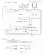
Hi luxury54,
I added a concept diagram of the SD-card player, it includes a dynamic jitter reduction circuit for BCK. Photograph of the working prototype was recently posted.
The master clock is a simplified version of the 12-crystal master clock that is going to be used in the TDA1541A-based SD-player. These master clocks use a tuned crystal filter (3rd ... 12th order) This filter is used for both the oscillation and for filtering the output signal. This way very clean sine waves with low distortion can be obtained.
Since mains-powered reference voltages would be way too noisy, I used a 1.5V alkaline reference voltage instead. The power supply (5V) is less critical. The master clock now performs like if it was running on a clean battery power supply, while barely consuming any power from the battery reference voltage (150nA max.).
The master clock is built around a discrete HF buffer with high input impedance. This buffer is powered by a constant current source. It also has dual discrete HF output buffers that were specifically designed to avoid any frequency shift due to capacitive loading, thus isolating the master clock from connected loads. This helps to maintain extreme low jitter levels with varying loads
The digital audio source is a SD-card player. The SD(HC) memory card is read by a dsPIC controller, and the data is converted to I2S by an on-chip DCI module. There is a separate display controller that also divides the master clock by 2 (required for this application).
The dsPIC BCK output signal (1.4112 MHz) is fed to a fast single D flip-flop (160MHz ... 4GHz), synchronously reclocking BCK with the master clock, using a dedicated clean buffered output. This provided best audible results (jitter is already too low to measure with my test equipment), it was much better than using a synchronous divider (divide-by-8).
The already extremely low jitter is further attenuated in the dynamic jitter attenuation circuit. This circuit mainly tackles the lower jitter frequency spectrum (this is a problematic range for crystal oscillators).
The Schottky diodes perform clock signal interruption below TDA1543 digital input bias voltage, this greatly reduces interference. The attenuated clock signal appears across the 150 Ohm resistor. The clock signal also drives an integrator, composed of 220nF and 490 Ohm (approx. values). The integrator derives an average bias voltage that fluctuates with the master clock duty cycle (jitter) and thus manipulates the bias voltage. This determines the exact moment the TDA1543 output latch triggers. The required corrections are extremely small.
This means that BCK still has certain jitter amplitude, but the DAC sample timing jitter would have dropped. This configuration integrates both source and DAC, this enables very high performance and completely eliminates interface / interlink issues.
Unlike many transport / DAC combinations (external DACs), this player only has one clock source (single time domain) and one related clock jitter spectrum. This turned out to be crucial for optimal performance.
Both DATA and WS signals have a resistive I2S attenuator, a choke is added to attenuate power supply noise. The attenuators are required to achieve a clean analog output signal, without them, sound quality degrades significantly (sound smearing).
Same applies for Vref (pin7) if this pin is connected to anything, sound quality degrades dramatically. This is caused by ground or power supply noise polluting both bias current source and DAC output current, then it's over. So never ever connect this pin!
Same applies for paralleling multiple TDA1543, this will increase interference levels and jitter amplitude. If multiple TDA1543 chips must be used in a design (balanced DAC), they must be completely separated and have separate attenuated I2S signals. Even then it's very difficult to maintain low jitter and I2S interference levels.
I use 680 Ohm passive I/V resistors, this gives enough signal to directly drive my power amps (100K input impedance). Since I only use one TDA1543, I need a reference voltage for these I/V resistors. This is also required to use the actual DAC output current (that flows to GND).
Mains power supplies are too polluted for this, and a "floating" supply is required. So I simply used 2 penlight alkaline batteries (I needed one for the master clock anyway). Current consumption (TDA1543 powered-up) equals 2 x 1.15mA = 2.3mA. When the player is shut-down, the TDA1543 no longer draws any bias current, so the battery can simply stay connected. The master clock only consumes a few hundred nano amperes when shut down, and even less when operating. So the batteries should last a long time.
Despite grossly exceeding datasheet 25mV output compliance, distortion stays low (checked with a Marconi distortion meter). I also tried other I/V converters, including the trans-impedance converter, and a fast Op-amp. The passive I/V converter clearly performed best with this chip, so that's why I used it.
The SD-card digital audio source generates Philips I2S with 32 bits / frame, this provides a continuous data stream without periodic interruptions like with 64 bits / frame. This provides two advantages, first the bit clock frequency can be halved (less ground bounce), and second, the DATA flow is more fluid, causing less interference.
At the bottom is the block diagram showing the highly criticized volume control.
I'm very curious about your further improvement in the I2S jitter reduction circuit and how would it behave in a CD-player integrated DAC...would it be possible to give some more info on this?
I added a concept diagram of the SD-card player, it includes a dynamic jitter reduction circuit for BCK. Photograph of the working prototype was recently posted.
The master clock is a simplified version of the 12-crystal master clock that is going to be used in the TDA1541A-based SD-player. These master clocks use a tuned crystal filter (3rd ... 12th order) This filter is used for both the oscillation and for filtering the output signal. This way very clean sine waves with low distortion can be obtained.
Since mains-powered reference voltages would be way too noisy, I used a 1.5V alkaline reference voltage instead. The power supply (5V) is less critical. The master clock now performs like if it was running on a clean battery power supply, while barely consuming any power from the battery reference voltage (150nA max.).
The master clock is built around a discrete HF buffer with high input impedance. This buffer is powered by a constant current source. It also has dual discrete HF output buffers that were specifically designed to avoid any frequency shift due to capacitive loading, thus isolating the master clock from connected loads. This helps to maintain extreme low jitter levels with varying loads
The digital audio source is a SD-card player. The SD(HC) memory card is read by a dsPIC controller, and the data is converted to I2S by an on-chip DCI module. There is a separate display controller that also divides the master clock by 2 (required for this application).
The dsPIC BCK output signal (1.4112 MHz) is fed to a fast single D flip-flop (160MHz ... 4GHz), synchronously reclocking BCK with the master clock, using a dedicated clean buffered output. This provided best audible results (jitter is already too low to measure with my test equipment), it was much better than using a synchronous divider (divide-by-8).
The already extremely low jitter is further attenuated in the dynamic jitter attenuation circuit. This circuit mainly tackles the lower jitter frequency spectrum (this is a problematic range for crystal oscillators).
The Schottky diodes perform clock signal interruption below TDA1543 digital input bias voltage, this greatly reduces interference. The attenuated clock signal appears across the 150 Ohm resistor. The clock signal also drives an integrator, composed of 220nF and 490 Ohm (approx. values). The integrator derives an average bias voltage that fluctuates with the master clock duty cycle (jitter) and thus manipulates the bias voltage. This determines the exact moment the TDA1543 output latch triggers. The required corrections are extremely small.
This means that BCK still has certain jitter amplitude, but the DAC sample timing jitter would have dropped. This configuration integrates both source and DAC, this enables very high performance and completely eliminates interface / interlink issues.
Unlike many transport / DAC combinations (external DACs), this player only has one clock source (single time domain) and one related clock jitter spectrum. This turned out to be crucial for optimal performance.
Both DATA and WS signals have a resistive I2S attenuator, a choke is added to attenuate power supply noise. The attenuators are required to achieve a clean analog output signal, without them, sound quality degrades significantly (sound smearing).
Same applies for Vref (pin7) if this pin is connected to anything, sound quality degrades dramatically. This is caused by ground or power supply noise polluting both bias current source and DAC output current, then it's over. So never ever connect this pin!
Same applies for paralleling multiple TDA1543, this will increase interference levels and jitter amplitude. If multiple TDA1543 chips must be used in a design (balanced DAC), they must be completely separated and have separate attenuated I2S signals. Even then it's very difficult to maintain low jitter and I2S interference levels.
I use 680 Ohm passive I/V resistors, this gives enough signal to directly drive my power amps (100K input impedance). Since I only use one TDA1543, I need a reference voltage for these I/V resistors. This is also required to use the actual DAC output current (that flows to GND).
Mains power supplies are too polluted for this, and a "floating" supply is required. So I simply used 2 penlight alkaline batteries (I needed one for the master clock anyway). Current consumption (TDA1543 powered-up) equals 2 x 1.15mA = 2.3mA. When the player is shut-down, the TDA1543 no longer draws any bias current, so the battery can simply stay connected. The master clock only consumes a few hundred nano amperes when shut down, and even less when operating. So the batteries should last a long time.
Despite grossly exceeding datasheet 25mV output compliance, distortion stays low (checked with a Marconi distortion meter). I also tried other I/V converters, including the trans-impedance converter, and a fast Op-amp. The passive I/V converter clearly performed best with this chip, so that's why I used it.
The SD-card digital audio source generates Philips I2S with 32 bits / frame, this provides a continuous data stream without periodic interruptions like with 64 bits / frame. This provides two advantages, first the bit clock frequency can be halved (less ground bounce), and second, the DATA flow is more fluid, causing less interference.
At the bottom is the block diagram showing the highly criticized volume control.
Attachments
Same applies for paralleling multiple TDA1543, this will increase interference levels and jitter amplitude. If multiple TDA1543 chips must be used in a design (balanced DAC), they must be completely separated and have separate attenuated I2S signals. Even then it's very difficult to maintain low jitter and I2S interference levels.
But every time you double the devices in parallel you reduce the noise floor by 3dB
Hi jameshillj,
This might be interesting, when I read it, I thought "this can't work". Yet curious as I am, I just tried it for myself. I am still glad I did.
http://www.altmann.haan.de/splif_page/
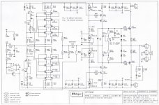
I use home-made, fully complementary cascoded-cascode power amps. These have local feedback (not affected by back-emf from the speakers).
I attached a schematic diagram of this amplifier. It runs on a single power supply and has floating GND. The input is DC-coupled, so the 1uF coupling cap is the only cap in the signal path between DAC and amplifier.
Other nice detail, most speakers already have resistive attenuators installed (midrange / tweeter) to achieve flat frequency response.
I also use home made sonic resonators. These have an integrated element that performs real-time dynamic corrections (woofer / low-midrange). This way a flat impedance curve is obtained, and the woofer / midrange speaker chassis are kept under tight control.
I already tried with high DAC output voltage (up to approx. 70Vpp), but the problem is DAC output power, in order to generate these signal amplitudes, and have enough power to reliably drive a buffer, higher DAC output current is required. This is not very practical as it requires multiple DAC chips that introduce new problems.
Possible option is varying power amplifier gain, this can be done, but is very tricky (bandwidth increases with lower gain). It also won't attenuate noise, hum and amplifier cross-over distortion like the external attenuator would.
in short, the amplifier and speaker are a SYSTEM and work together because of the difficult and varying speaker parameters that change with driver impedance, power, freq, phase, transient_ response, compression, Xover, etc,_ plus the amps ability to control the back emf and avoid loading the neg feedback networks, output stage damping, etc, etc.___ Adding a FIXED value resistive attenuator network into the middle of this is a relatively simple thing (driver eq) but even this produces unexpected complications_ and so a full freq range, varyible load attenuator will introduce enormous difficulties (even with a reduced operating volume range), particularly with very high quality sound reproduction. __ Perhaps it would be better to use this higher voltage output from the DAC and adjust the gain of the amplifier for the required volume or perhaps a higher voltage attenuator with an output power buffer - a much simpler thing to do.
This might be interesting, when I read it, I thought "this can't work". Yet curious as I am, I just tried it for myself. I am still glad I did.
http://www.altmann.haan.de/splif_page/
I use home-made, fully complementary cascoded-cascode power amps. These have local feedback (not affected by back-emf from the speakers).
I attached a schematic diagram of this amplifier. It runs on a single power supply and has floating GND. The input is DC-coupled, so the 1uF coupling cap is the only cap in the signal path between DAC and amplifier.
Other nice detail, most speakers already have resistive attenuators installed (midrange / tweeter) to achieve flat frequency response.
I also use home made sonic resonators. These have an integrated element that performs real-time dynamic corrections (woofer / low-midrange). This way a flat impedance curve is obtained, and the woofer / midrange speaker chassis are kept under tight control.
I already tried with high DAC output voltage (up to approx. 70Vpp), but the problem is DAC output power, in order to generate these signal amplitudes, and have enough power to reliably drive a buffer, higher DAC output current is required. This is not very practical as it requires multiple DAC chips that introduce new problems.
Possible option is varying power amplifier gain, this can be done, but is very tricky (bandwidth increases with lower gain). It also won't attenuate noise, hum and amplifier cross-over distortion like the external attenuator would.
Attachments
Hi yygomez,
True, but two DAC chips also produce more interference. Then there is the doubled clock load (BCK).
The master clock in the SD player has two discrete HF clock buffers that each drive a single load. It's that critical, I couldn't even connect two loads to one buffered clock output without causing increased timing jitter levels.
Multiple DAC chips can be used, but it's tricky to keep interference levels low enough, and maintain lowest possible timing jitter.
But every time you double the devices in parallel you reduce the noise floor by 3dB
True, but two DAC chips also produce more interference. Then there is the doubled clock load (BCK).
The master clock in the SD player has two discrete HF clock buffers that each drive a single load. It's that critical, I couldn't even connect two loads to one buffered clock output without causing increased timing jitter levels.
Multiple DAC chips can be used, but it's tricky to keep interference levels low enough, and maintain lowest possible timing jitter.
maxlorenz said:
Given that, why nobody challenged the following statement?
http://www.firstwatt.com/downloads/cs-amps-speakers.pdf
Probably because Nelson Pass makes it clear that his remarks apply only to a small group of loudspeaker drivers: "As I said, most speakers are designed around voltage sources but there are a few instances where a current source can be used to advantage".
jonners said:
Probably because Nelson Pass makes it clear that his remarks apply only to a small group of loudspeaker drivers: "As I said, most speakers are designed around voltage sources but there are a few instances where a current source can be used to advantage".
Max, on exactly which portion of the 30 page article, including extensive measurements of real world drivers, would you be inclined to challenge Nelson?
the same article also stated:
Tube amplifiers seem to bring out the best in such (high efficiency / full range ) drivers. They have more bottom end, a
warmer, mellower mid and upper mid-range, and often more top octave. By comparison, the “best” solid-state state amplifiers make them sound more like transistor radios – less bottom and a, occasionally strident upper midrange.
If you are a solid-state kind of guy (like me) you start wondering how that could be, and if you are a tube aficionado, you smirk and say, “I told you so.”
The solid-state guy probably starts fixing the response with a parametric equalizer, and the tube guy enjoys his music with a nice glass of wine.
papa's definitely got a sense of humor
chrisb said:
Max, on exactly which portion of the 30 page article, including extensive measurements of real world drivers, would you be inclined to challenge Nelson?
I don't think Max wants to challenge Nelson! ( Do you Max? )
I think Max is asking why, when Nelson P and John/EC are saying essentially the same thing, ...why are people challenging the latter but not the former?
I'm just pointing out that NP makes it clear that he is referring to a small, specialised class of drivers. That makes it hard to disagree with what he is saying.
Hi ECThe master clock in the SD player has two discrete HF clock buffers that each drive a single load. It's that critical, I couldn't even connect two loads to one buffered clock output without causing increased timing jitter levels.
How do you measure timing Jitter levels?
- Home
- Source & Line
- Digital Line Level
- Building the ultimate NOS DAC using TDA1541A