When the DAC output current is (almost) zero, T1 might go out of conduction. This must be compensated by adding a very clean and constant current from TDA1541A output to -5 volts. Practical value is around 0.4mA.
For the TDA 1541A, Just wonder if I need to add any current sources to avoid DAC output current is zero? Under what condition will the 1541A output current is zero ?
ccschua said:Hi ECDesigns
The problem is the DC voltage at C2 input is 8.1V DC and the output is droping from 8.9V to about 300mV, and it takes about 4 minutes to drop to 300mV. With that output DC so high, I cant connect it to my amp.
ccschua said:
For the TDA 1541A, Just wonder if I need to add any current sources to avoid DAC output current is zero? Under what condition will the 1541A output current is zero ?
Hope you don't mind if I reply 😀
If you measure with nothing connected after C2 you are not providing a return path for the current so C2 doesn't get charged. Try connecting a 100-470k resistor to gnd and you will measure correct voltages.
The "output" current for the TDA1541A varies from 0 to -4mA (remember it sinks current) so at full scale it will sink 4mA and at -full scale it won't sink anything (maybe it's the opposite but the concept is the same).
When sinking 4mA voltage drop on R1 will be 6V so T1 still works fine.
When sinking 0mA the TDA will be perfectly fine but T1 will switch off, unless you provide additional current request (the 0.4mA....). This is the situation you have to avoid.
To do so you need a CCS (or a resistor.. pick your poison) and a negative voltage, since the Iout node sits at 0V.
This "residual" current also prevents T2's base from hitting the rail voltage and becoming saturated.
Ciao
Andrea
I am sorry, I dont really know what CCS stands for. I am so ignorant.
How to implement -5V with the -0.4mA draw ? by doing so, isnt that the output is short of the 0,4mA ?
How to implement -5V with the -0.4mA draw ? by doing so, isnt that the output is short of the 0,4mA ?
Hi, CCS stands for Constant Current Source (or Sink).
The simplest solution I can think of can be a Jfet CCS or a J502...
This current is constant and translates in a slightly different operating point for T1 and T2 but doesn't influence the signal from the DAC.
Ciao
Andrea
The simplest solution I can think of can be a Jfet CCS or a J502...
This current is constant and translates in a slightly different operating point for T1 and T2 but doesn't influence the signal from the DAC.
Ciao
Andrea
ccschua -
This schematic shows the idea: Q4 is the current source, connected between the i-DAC output and -15V. http://www.diyaudio.com/forums/attachment.php?s=&postid=103883&stamp=1041245775
This schematic shows the idea: Q4 is the current source, connected between the i-DAC output and -15V. http://www.diyaudio.com/forums/attachment.php?s=&postid=103883&stamp=1041245775
This is what I can think of.
First I put a 100K resistor at the output of C2. I do measure almost 0V dc now.
Then I intend to use -12V with the R4 at 30k to give a current sink of 0.4mA. ( I am assuming the Idac point is 0V dc.

First I put a 100K resistor at the output of C2. I do measure almost 0V dc now.
Then I intend to use -12V with the R4 at 30k to give a current sink of 0.4mA. ( I am assuming the Idac point is 0V dc.
Sorry If I'm being dense - aren't the data sheet noise given over a defined bandwidth?
You're correct, sorry my mistake.
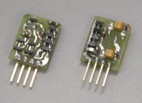
Meanwhile the new voltage regulator modules for the D1M were completed. I attached a photograph of these compact regulators showing both component and solder side. The regulators consist of a capacitance multiplier using a triple-darlington, a constant current source, also based on a triple-darlington, an external 10mH choke, and finally a shunt-regulator, based on 8 x TS431 in parallel. The modules are intended for low output currents (up to approx. 100mA). I use multiple of these regulators in the D1M, output voltages are set at 3.3 or 5 Volts.
Can we take the approach to regenerate the I2S by buffering the data and recreate it? The idea is same as playoff delay buffer used in VOIP.
Regarding digital audio source for high-performance audio, there is one almost perfect solution:
- Swappable semiconductor memory holding uncompressed WAV files.
- Digital audio source located in the DAC (no USB or SPDIF Coax / Toslink interfaces required).
- Digital audio source runs on the low-jitter masterclock.
- Digital audio source outputs I2S.
My brother is currently working on this solution, and if all goes well, the D1M will soon have an integrated music player and even better sound quality.
Regarding PLL in the USB chip.
That's why I use the AE module that only has one connected USB load that gets highest priority, all the time.
Kindly check if the R2, R3 value is correct or need to be replaced. C2 is 4u7.
They are correct, but you must connect a resistive load (passive volume control) from output to GND, 47 ... 100 K Ohm for example. This is required for charging C2, if C2 can't be charged, DC will appear at the output.
When sinking 4mA voltage drop on R1 will be 6V so T1 still works fine.
When sinking 0mA the TDA will be perfectly fine but T1 will switch off, unless you provide additional current request (the 0.4mA....). This is the situation you have to avoid
When the TDA1541A sinks current, the transistor will conduct. When the TDA1541A output current drops to zero, T1 will stop conducting, but since the DAC output current is zero, there is no need for T1 to conduct, as there is no DAC current to pass to the I/V resistor.
I have removed both constant current sources from the D1M trans-impedance converter as they clearly degrade perceived sound quality. This became very clear after installing the new low-noise power supply modules.
The simplest solution I can think of can be a Jfet CCS or a J502...
These have become obsolete, and are rather unsuitable for this application, since the resulting output current is far from constant. For this application the constant current must be very clean without the slightest pollution (LSB change results in approx. 61nA). So the "lesser evil" is leaving out the bias current all together.
This schematic shows the idea: Q4 is the current source, connected between the i-DAC output and -15V
The one-transistor current source, like the J502 is also unsuitable for this kind of demanding applications. All I can suggest is to forget about using constant current sources here.
Attachments
-ecdesigns- said:
Regarding digital audio source for high-performance audio, there is one almost perfect solution:
- Swappable semiconductor memory holding uncompressed WAV files.
- Digital audio source located in the DAC (no USB or SPDIF Coax / Toslink interfaces required).
- Digital audio source runs on the low-jitter masterclock.
- Digital audio source outputs I2S.
My brother is currently working on this solution, and if all goes well, the D1M will soon have an integrated music player and even better sound quality.
This sounds amazing! - What form will the semiconductor memory take, and how do you get your digital info - CDs etc.- into that form? Will you start a new thread on this? 😎
Hi John,
Do you have any pcbs for sale that would let me build one of the earlier DACs based on 4 x TDA1541 chips. I have a reclocked I2S signal, so would only be looking for the DAC chip modules, Interpolation module PS and I/V stage.
I am getting my head around what you were doing with this project at the end of 2007, and just cannot keep up - I think that the DAC based on the 4 TDA1541s, with the more recent updates would be a good point for me to dive into this.
I don't mind re-working some of the boards that you do have, to make the most of the recent updates.
Brad
Hi jonners,
Semiconductor memory will probably be a SD memory card (up to 32 Gb capacity).
WAV files can be stored on the SD memory card using a computer. We decided to use FAT32 file system in order to support larger SD-card capacities.
The SD-card player DSP reads the WAV file from the SD card and uses on-chip hardware (DMA / dual-ported RAM / buffers / I2S generation logic) to produce an I2S output stream.
Both DSP and DAC chip share the same master clock. The DSP has on-chip clock divider and clock multiplier to generate required on-chip clock frequency.
There is still a lot to sort out, and this will take quite some time. When time comes, I could start a new thread for it.
This sounds amazing! - What form will the semiconductor memory take, and how do you get your digital info - CDs etc.- into that form? Will you start a new thread on this?
Semiconductor memory will probably be a SD memory card (up to 32 Gb capacity).
WAV files can be stored on the SD memory card using a computer. We decided to use FAT32 file system in order to support larger SD-card capacities.
The SD-card player DSP reads the WAV file from the SD card and uses on-chip hardware (DMA / dual-ported RAM / buffers / I2S generation logic) to produce an I2S output stream.
Both DSP and DAC chip share the same master clock. The DSP has on-chip clock divider and clock multiplier to generate required on-chip clock frequency.
There is still a lot to sort out, and this will take quite some time. When time comes, I could start a new thread for it.
Hi Builder Brad,
I still have the following PCBs that could be interesting for experimenting:
- DI8 mainboard
- TDA1541A PCB
- I/V converter PCB
- Interpolator PCB
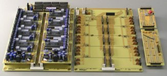
I attached a photograph of the mainboard that can hold up to 8 TDA1541A modules, the interpolator, and 2 I/V converter PCBs.
Do you have any pcbs for sale that would let me build one of the earlier DACs based on 4 x TDA1541 chips. I have a reclocked I2S signal, so would only be looking for the DAC chip modules, Interpolation module PS and I/V stage.
I still have the following PCBs that could be interesting for experimenting:
- DI8 mainboard
- TDA1541A PCB
- I/V converter PCB
- Interpolator PCB
I attached a photograph of the mainboard that can hold up to 8 TDA1541A modules, the interpolator, and 2 I/V converter PCBs.
Attachments
When the TDA1541A sinks current, the transistor will conduct. When the TDA1541A output current drops to zero, T1 will stop conducting, but since the DAC output current is zero, there is no need for T1 to conduct, as there is no DAC current to pass to the I/V resistor.
I measure the IDAC point and found the DC voltage about 140mV. I guess this is above the 25mV required at the Idac output (virtual ground). I measure the ground it is 0.5mV dc.
I found the transimpedance working properly now. I work on the project board for 1 channel but when I put in the other chanell, the noise appear at the other channel. I suspect because I need to build another power supply of 12V for supplying the other channel right ? Putting the other channel increase the ground voltage to 1.5mV.

Hi John,
On post #2647 and #2651, you outlined an idea for using a SD Memory card for downloading info from a computer - could this be done using a system similar to your Charge Transfer power supply technique sending smaller "packets" of WAV files to a connected RAM memory and then further transferring them onto another RAM tied to the DAC this time and then onto the outlined I2S coding system?
Also, is there any dis/advantages in using perhaps a LM334z (noise, regulation, ripple, etc?) instead of the TL431 used throughout the power supplies?
And finally, would it be possible to supply that bias 0.4mA to the 1541A O/P pin with a battery supply (yuck!) and regulator?
So I separated the power (by bringing 2 wires of 12V) to two separate rail for the transimpedance circuit. Now the ground is manageable at 0.8mV for both circuit (balanced now, with reference to the starpoint ground at the DAC board).
However I cant get away with the Idac point of DC offset. it is still at 150mV. Next I install the C2240 (both Collector and Base shorted) to replace the 1N4148. I notice the DC offset drops but it is still way above the 25mV. (it is about 120mV)
Is there an output impedance at the Idac that causes it to pull up to 150mV ?
[Listening test shows the transimpedance circuit is better than the opamp using 5532, however it is still quite a distance from my heavily modded cd63 with blackgate ]
Hi John,
Those items are exactly what I am looking for, at least I will get to hear the Direct Interpolation in action.
I have a couple of questions:
how much do you want for the boards?, pls send a private msg if you prefer.
Are the SMD parts already soldered to the boards?
Brad
Those items are exactly what I am looking for, at least I will get to hear the Direct Interpolation in action.
I have a couple of questions:
how much do you want for the boards?, pls send a private msg if you prefer.
Are the SMD parts already soldered to the boards?
Brad
hello all,
for those of you who made the DEM reclocking using 352 khz + the inverted 352 khz signal on pins 16,17 i have 1 small question:
I made a low jitter kwak clock 7 ,which i fed to a 74HCT4040 to divide and generate that 352 khz and after that this goes to an inverter (the 74HC04) for the inverted generation of the 352 khz.
So my question would be - since the AD8561 comparator from the KWAK CLOCK 7 board is outputing also inverted clock signal of 11.8296 mhz (but it's not used) could i use instead of that 74HC04 inverter another 74HCT4040 divider chip fed by the inverted master clock signal of the KWAK CLOCK to generate the inverted 352 khz DEM signal?
I think that it might have a lower jitter coming direct from master clock instead of using a separate inverter after the division
some advices are welcome,thanks !
luxury54 said:hello all,
since the AD8561 comparator from the KWAK CLOCK 7 board is outputing also inverted clock signal of 11.8296 mhz (but it's not used) could i use instead of that 74HC04 inverter another 74HCT4040 divider chip fed by the inverted master clock signal of the KWAK CLOCK to generate the inverted 352 khz DEM signal?
some advices are welcome,thanks !
Why not just try it. u need both 352kHz and inverted signal to go into pin 16,17 of TDA1541, before the pin, u need the resistor and capacitor.
I try replacing R3 which is 510R to 1k. Now the Idac dc voltage is now 20mV which is better. However I found the resistor to be very which puzzle me. Since power = square (V) / R. by putting a bigger R, isnt that the power dissipation is smaller. Putting the 1k resistor also raises the ground to about 2mV. ? what cause it so hot??
I am still left with the output DC to adjust to zero. Is it I need perfectly matched T1 ? what measurement is that , hfe ?
I am still left with the output DC to adjust to zero. Is it I need perfectly matched T1 ? what measurement is that , hfe ?
Hi Luxury54,
I am currently using the 74hc4040 to generate the 352khz for DEM reclocking, and then using an 074 chip to invert the signal. I think that you would be better taking out the 074 chip from the circuit if you have an inverted source clock, and then sending that to another 74hc4040 chip.
There was also a suggestion in an earlier post by Onnosr (post 2532) to use a diferential line driver chip DS8941, that looks like an even better solution.
Brad
- Home
- Source & Line
- Digital Line Level
- Building the ultimate NOS DAC using TDA1541A