I'm afraid that the LM337 might not be the best choice for CCS, especially with the high-frequencies at the output of the DAC.
I'd rather use a cascoded JFET or a BJT CCS...
Ciao
Andrea
I'd rather use a cascoded JFET or a BJT CCS...
Ciao
Andrea
Andypairo said:I'm afraid that the LM337 might not be the best choice for CCS, especially with the high-frequencies at the output of the DAC.
I'd rather use a cascoded JFET or a BJT CCS...
Ciao
Andrea
We seem to forget, that in that position, a simple resistor, does the job as well. Measured on the bench it will be beaten, but sound wise there is not always a need for a CCS if a resistor can do the job. The input impedance of the common base is low enough to determine the ac load for the dac current output, so a relative high DC Bias resistor sits nicely there
Hi maxlorenz,
If you connect 4 trans-impedance converters, you end up with 2 differential outputs for each channel that only have slight relative DC-offset. This might work with a TVC, it won't work when driving an XLR input. Problems might occur during power-up / down, or when the master clock stops. The last sample will then be output continuously, causing a permanent DC voltage between both outputs. If this happens, the TVC core gets saturated / magnetized immediately.
The main parameters affecting DC output voltage are I/V resistor tolerance, TDA1543 tolerances, and transistor Vbe tolerances. I personally would always add a coupling cap for safety.
I suspect that if I connect each DAC output (NIR, NIL, IR, IL) to its corresponding trans impedance/buffer circuit I could end with a balanced output NOS DAC, and, as I use a TVC as preamp.
If you connect 4 trans-impedance converters, you end up with 2 differential outputs for each channel that only have slight relative DC-offset. This might work with a TVC, it won't work when driving an XLR input. Problems might occur during power-up / down, or when the master clock stops. The last sample will then be output continuously, causing a permanent DC voltage between both outputs. If this happens, the TVC core gets saturated / magnetized immediately.
I could get rid of the output caps, since all the trans impedance circuits will be fed by the same power supply, so I hope DC output will cancel out on the transformer based preamp...am I right?
(using matched parts and transistors, that is...)
The main parameters affecting DC output voltage are I/V resistor tolerance, TDA1543 tolerances, and transistor Vbe tolerances. I personally would always add a coupling cap for safety.
Hi JC951t
The published trans-impedance converter only requires transistor T1 to be driven into full saturation. This requires a small constant current flowing from DAC output to GND (TDA1543) or to -5V (TDA1541A).
The circuit requires a very clean power supply, but this basically applies to all circuits used in a DAC.
I can only say, keep the circuit as simple as possible, use the best components you can find, and think twice before adding any unnecessary parts in the signal path.
Question. Would biasing the transimpedance circuit
for a parallel TDA 1541 be of any benefit sound wise ?
The published trans-impedance converter only requires transistor T1 to be driven into full saturation. This requires a small constant current flowing from DAC output to GND (TDA1543) or to -5V (TDA1541A).
The circuit requires a very clean power supply, but this basically applies to all circuits used in a DAC.
I can only say, keep the circuit as simple as possible, use the best components you can find, and think twice before adding any unnecessary parts in the signal path.
Hi ccschua,
No, the TDA1541A full-scale output current equals approx. 4 mA. Bias current equals approx. 2mA. So the DAC AC output current varies between approx. zero and 4mA when processing digital audio data.
Using 1K4 I/V resistor as an example, the minimum voltage across the resistor will be zero volts, the maximum voltage would be 0.004 * 1400 = 5.6 volts. The average (DC) voltage across the I/V resistor will be 0.002 * 1400 = 2.8 Volts. Since the I/V resistor is connected to +12V, the actual voltage across R1 equals 12V - V(R1).
Using the same example, V(R1) varies between 12V and 6.4V. The average (DC) voltage equals 12V - 2.8V = 9.2V. The output buffer causes approx. 0.6V additional voltage drop, changing the values to 11.4 (DAC output current = 0), 8.6V (DAC average DC output current), and 5.8V (DAC output current equals 4mA).
The output coupling cap C2 will block DC voltages, so an AC voltage with maximum amplitude of 6.4Vpp will be created at the converter output.
When the DAC output current is (almost) zero, T1 might go out of conduction. This must be compensated by adding a very clean and constant current from TDA1541A output to -5 volts. Practical value is around 0.4mA.
The AC signal of 5.6Vpp (example) is created by the varying AC DAC output current through the I/V resistor. Since the DAC current keeps varying with the audio signal, an AC voltage will be created directly across the passive I/V resistor R1.
So does this mean that TDA1541a draws min 2mA. and it swings from 2mA to 4mA to give the corresponding ac signal.
No, the TDA1541A full-scale output current equals approx. 4 mA. Bias current equals approx. 2mA. So the DAC AC output current varies between approx. zero and 4mA when processing digital audio data.
Using 1K4 I/V resistor as an example, the minimum voltage across the resistor will be zero volts, the maximum voltage would be 0.004 * 1400 = 5.6 volts. The average (DC) voltage across the I/V resistor will be 0.002 * 1400 = 2.8 Volts. Since the I/V resistor is connected to +12V, the actual voltage across R1 equals 12V - V(R1).
Using the same example, V(R1) varies between 12V and 6.4V. The average (DC) voltage equals 12V - 2.8V = 9.2V. The output buffer causes approx. 0.6V additional voltage drop, changing the values to 11.4 (DAC output current = 0), 8.6V (DAC average DC output current), and 5.8V (DAC output current equals 4mA).
The output coupling cap C2 will block DC voltages, so an AC voltage with maximum amplitude of 6.4Vpp will be created at the converter output.
When the DAC output current is (almost) zero, T1 might go out of conduction. This must be compensated by adding a very clean and constant current from TDA1541A output to -5 volts. Practical value is around 0.4mA.
Now since the DC is blocked by the coupling cap C2, where does this AC signal come from to give an output of 2V PP for driving the audio amp?
The AC signal of 5.6Vpp (example) is created by the varying AC DAC output current through the I/V resistor. Since the DAC current keeps varying with the audio signal, an AC voltage will be created directly across the passive I/V resistor R1.
Hi Andypairo,
Yes, the LM337 is not the best choice here (to much noise, poor regulation at higher frequencies).
I use a bipolar low noise transistor, fed by a 1.25V precision voltage reference, connected to another 2.7V precision voltage reference (double regulation). The CCS also has integrated HF compensation for improved stability over a large bandwidth.
The converter must also run on a super clean power supply (just like all other DAC sub-circuits). I am now testing hybrid voltage regulators:
Capacitance multiplier > low-pass filter > precision constant current source > LC lowpass filter > shunt regulator.
Separate hybrid voltage regulators are used to power each sub-circuit of the D1M. These hybrid power supplies are fed by a discrete series regulator.
The D1M is powered externally using the new floating CT power supply, and built-in capacitance multiplier.
I'm afraid that the LM337 might not be the best choice for CCS, especially with the high-frequencies at the output of the DAC.
I'd rather use a cascoded JFET or a BJT CCS...
Yes, the LM337 is not the best choice here (to much noise, poor regulation at higher frequencies).
I use a bipolar low noise transistor, fed by a 1.25V precision voltage reference, connected to another 2.7V precision voltage reference (double regulation). The CCS also has integrated HF compensation for improved stability over a large bandwidth.
The converter must also run on a super clean power supply (just like all other DAC sub-circuits). I am now testing hybrid voltage regulators:
Capacitance multiplier > low-pass filter > precision constant current source > LC lowpass filter > shunt regulator.
Separate hybrid voltage regulators are used to power each sub-circuit of the D1M. These hybrid power supplies are fed by a discrete series regulator.
The D1M is powered externally using the new floating CT power supply, and built-in capacitance multiplier.
LM317
Hi all,
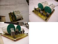
I know that a LM317 is not the best choice, but it is only a test pcb to hear what can the TDA1541A do, I'm designing the second pcb. This last will be much better. When I have finished it I'll post a photo. Respect to the LM317 one, I've tested it yesterday, and the sound is very very good. Very clean, detailed, exceptional dynamics, etc....
Designing a good power supply has some work, because it has a lot of components. That why I decided to design first a simple output pcb and try it with a digilog from Musical Fidelity (of a friend, it's not mine). The next step is to bypass the SAA7020, and change all capacitors, and rectifiers and try it.
I highly apreciate your oppinions, thank you all.
regards,
Hi all,
I know that a LM317 is not the best choice, but it is only a test pcb to hear what can the TDA1541A do, I'm designing the second pcb. This last will be much better. When I have finished it I'll post a photo. Respect to the LM317 one, I've tested it yesterday, and the sound is very very good. Very clean, detailed, exceptional dynamics, etc....
Designing a good power supply has some work, because it has a lot of components. That why I decided to design first a simple output pcb and try it with a digilog from Musical Fidelity (of a friend, it's not mine). The next step is to bypass the SAA7020, and change all capacitors, and rectifiers and try it.
I highly apreciate your oppinions, thank you all.
regards,
Hi dddac,
The bias current needs to be approx. 0.4mA, the required resistor value would be 2.1 / 0.0004 = 5K25. This is a rather low impedance compared with a good CCS. You could use a -100V DC supply, this would give 102.1 / 0.0004 = 25K5, but this also won't provide much improvement.
The bias resistor would add a non-constant (approx. 0.4mA) current to the 2.3mA full-scale DAC output current (TDA1543), meaning that this current will vary with power supply fluctuations.
I tried resistors for adding required bias current, but unfortunately, the CCS resulted in clearly better perceived sound quality. So I had to add the CCS, despite the extra parts.
We need highest possible impedance here, so a suitable clean, large bandwidth CCS is preferred.
We seem to forget, that in that position, a simple resistor, does the job as well. Measured on the bench it will be beaten, but sound wise there is not always a need for a CCS if a resistor can do the job. The input impedance of the common base is low enough to determine the ac load for the dac current output, so a relative high DC Bias resistor sits nicely there
The bias current needs to be approx. 0.4mA, the required resistor value would be 2.1 / 0.0004 = 5K25. This is a rather low impedance compared with a good CCS. You could use a -100V DC supply, this would give 102.1 / 0.0004 = 25K5, but this also won't provide much improvement.
The bias resistor would add a non-constant (approx. 0.4mA) current to the 2.3mA full-scale DAC output current (TDA1543), meaning that this current will vary with power supply fluctuations.
I tried resistors for adding required bias current, but unfortunately, the CCS resulted in clearly better perceived sound quality. So I had to add the CCS, despite the extra parts.
We need highest possible impedance here, so a suitable clean, large bandwidth CCS is preferred.
-ecdesigns- said:Hi dddac,
The bias current needs to be approx. 0.4mA, the required resistor value would be 2.1 / 0.0004 = 5K25. This is a rather low impedance compared with a good CCS. You could use a -100V DC supply, this would give 102.1 / 0.0004 = 25K5, but this also won't provide much improvement.
The bias resistor would add a non-constant (approx. 0.4mA) current to the 2.3mA full-scale DAC output current (TDA1543), meaning that this current will vary with power supply fluctuations.
I tried resistors for adding required bias current, but unfortunately, the CCS resulted in clearly better perceived sound quality. So I had to add the CCS, despite the extra parts.
We need highest possible impedance here, so a suitable clean, large bandwidth CCS is preferred.
Hi EC,
I sure do not doubt your audible results, but just my 2 (facts) cents:
The input impedance of the Common Base is 16 Ohm. So 5k2 is quite high compared.
The extra current is pretty much constant. With 2.1 Volt only varying with the 10mV compliance, that is 0,5%
I do not understand why it fluctuates with the power supply? the 2,1 Volt is very stable, right?
So that makes me think, how come CCS sounds better? I will build a few versions myself to get a perception of the audible differences
take care
doede
Hi dddac,
When 25mVpp ouput compliance (0.0088 mVrms) is met, load impedance should be around 0.0088 / 0.0023 = 3.8 Ohms.
16 Ohm would result in 0.0023 * 16 = 36.8mVpp, this exceeds DAC chip output compliance.
The current running through the I/V resistor equals approx. (iDAC + IBias). IBias equals approx. 0.4mA, iDAC (full-scale equals approx. 2.3mA), so the impact of ibias on the generated output voltage across Riv is quite substantial despite common base circuit impedance.
Pretty much constant isn't enough. The 2.1 volts at the DAC output will fluctuate between approx. 2.10 and 2.11 volts (asuming 10mVpp AC voltage at DAC output that sits on 2.1 volts). Given the 5K2 bias resistor this translates to:
(2.11 / 5200) - (2.10 / 5200) = 0.00000193A or 1.92uA or 1902nA.
LSB change (2.3mA full-scale current) equals 0.0023 / 65536 = 0.000000035A or 35nA.
What actually happens is that the DAC output current is modulated with a non-constant bias current that varies with the DAC momentary output current. In short, non-linear distortion is added.
It both, measures, and sounds better due to lower non-linear distortion, see example. In addition, there is always interference (ripple / ground-bounce) on GND, however so small. Given the 3.8 Ohm impedance from the example, it only takes (0.0023 / 65536) * 3.8 = 0.000,000,133V or 133nV to mask LSB.
The input impedance of the Common Base is 16 Ohm. So 5k2 is quite high compared.
When 25mVpp ouput compliance (0.0088 mVrms) is met, load impedance should be around 0.0088 / 0.0023 = 3.8 Ohms.
16 Ohm would result in 0.0023 * 16 = 36.8mVpp, this exceeds DAC chip output compliance.
The current running through the I/V resistor equals approx. (iDAC + IBias). IBias equals approx. 0.4mA, iDAC (full-scale equals approx. 2.3mA), so the impact of ibias on the generated output voltage across Riv is quite substantial despite common base circuit impedance.
The extra current is pretty much constant. With 2.1 Volt only varying with the 10mV compliance, that is 0,5%
I do not understand why it fluctuates with the power supply? the 2,1 Volt is very stable, right?
Pretty much constant isn't enough. The 2.1 volts at the DAC output will fluctuate between approx. 2.10 and 2.11 volts (asuming 10mVpp AC voltage at DAC output that sits on 2.1 volts). Given the 5K2 bias resistor this translates to:
(2.11 / 5200) - (2.10 / 5200) = 0.00000193A or 1.92uA or 1902nA.
LSB change (2.3mA full-scale current) equals 0.0023 / 65536 = 0.000000035A or 35nA.
What actually happens is that the DAC output current is modulated with a non-constant bias current that varies with the DAC momentary output current. In short, non-linear distortion is added.
So that makes me think, how come CCS sounds better? I will build a few versions myself to get a perception of the audible differences
It both, measures, and sounds better due to lower non-linear distortion, see example. In addition, there is always interference (ripple / ground-bounce) on GND, however so small. Given the 3.8 Ohm impedance from the example, it only takes (0.0023 / 65536) * 3.8 = 0.000,000,133V or 133nV to mask LSB.
Hi EC,
Thanks for detailed feedback again. Just to make sure, the current through the transistor is aprox 1,5mA, so Ri is 16 Ohm
The requested Ri from 3,8 Ohm means a current of 6,6mA
I do take your point it would sound better and I will try things, but the point of masking LSB goes too far. There is noise coming from the CCS as well and from the 30k Internal impedance from the dac it self. On top, the TDA1543 has no 16 bit performance.
But the proof is in the eating
best
doede
Hi EC,
Thanks for your reply (post #2605) and for the following explanations...it sounds so easy as you explain it 🙂
Cheers,
M
Thanks for your reply (post #2605) and for the following explanations...it sounds so easy as you explain it 🙂
Cheers,
M
dddac said:On top, the TDA1543 has no 16 bit performance.
To be precise, it has 14 bit performance which equals the TDA1540.
dddac said:But the proof is in the eating
Bon appetit !

I2S signal amplitude
Hi EC
Thanks for sharing all of your knowledge with us. I have a couple of questions about your statement:
"In order to achieve lowest possible noise and bit clock jitter, the I2S signal amplitude at the DAC input MUST be as low as possible. In practice both chips that are based on current-steering logic, function reliably with 400mVpp I2S signal amplitude.
This greatly reduces ground-bounce, and lowers bit clock jitter inside the DAC chip at the clock input of the output latches where it really matters.
This basically applies to all external signals used in a DAC, try to minimize digital signal amplitude while ensuring reliable operation. Lowering signal amplitudes, results in much cleaner sound. It's also best to use correct impedance matching on all digital circuits. Directly connecting a TTL output to a TTL input doesn't provide optimal performance."
Is this true for any receivers feeding a TDA154X or just your new tracking receiver? I just built an AYAII and have 150R resistors between the CS8414 and the TDA1541. Should I reduce the signal further? Also I am feeding the CS8414 with a relatively high voltage AES signal. Do you recomend reducing the signal with resistors at the input of the CS8414, while preserving the impedance?
Thanks
JimS
Guys, you should really, really check-out EC's charge-transfer PS on amplifiers! 😎
Today I finished to mod two stereo UCD180 ClassD amps (without the gyrator part of the circuit) that feed my active Tannoy Autograph enclosures (Beyma coaxials) and the change in sound is astonishing.
Clean, clean (safe a buzz that always has anoyed me: the tweeter has 105db/W/m sensitivity; but this year I will tame it!) and detailed.
For this I bought power Mosfet and high current Schottkys, plus Panasonic TSHA (or THSA) 10000uF/63V caps for C1, which were the cheapest (but good) caps I found. The bass is deeper and more articulated, but the whole improvement is not at all like doubling the capacitance as I've done that before and I remember it was rather dissapointing.
So, instead of buying super expensive PS caps, I recommend buying regular industrial type and try EC's mod. 😉
Thanks John. 🙂
Sincerelly yours,
M
Hi Max,
Sounds good, why don't you make a sketch from what you actually did and post it ?
thanks !
doede
Sounds good, why don't you make a sketch from what you actually did and post it ?
thanks !
doede
Hi Doede,
I simply connected the "Mosfet type" or version 1 of the charge transfer PS to the existing rectifier bridge (yeah, I'm cheap); D3 is a Soft recovery rectifier diode and D4 is a high current Schottky whose number is longer than this thread...R4 connects to C2 and that is...just as in ecdesigns' diagram 🙂
http://picasaweb.google.com/lh/photo/rOgiSl8IVgPdqOcKLPkbNA?feat=directlink
Tell me if this did not help...cause I'm "at work" today with little spared time... 😀
Cheers,
M
- Home
- Source & Line
- Digital Line Level
- Building the ultimate NOS DAC using TDA1541A