EC,
it is common knowledge that tube buffers add pleasant harmonics. 😉
It is also common knowledge that the TDA1543 is an ultra-low performance & low budget & downgraded TDA1541 DAC chip that suffers from high DLE and will never ever sound clean.
It also has bad output voltage compliance & unipolar output current.
I wonder why you still use it.
There are other chips that would allow you to get away without any coupling caps, I2S attenuators, DEM reclockers, transimpedance inverters, active output buffers and whatever unnecessary stuff.
It should be clear that there is no coupling cap that will sound as neutral as a straight wire...
Same goes for transimpedance inverters & active output buffers. 😉
A negative post from you Bernard. Did you care to read why EC choose to use TDA1543 ? Or do you just want to express an opinion ?
There is no need to wonder as he nearly always chooses to express why he uses a topology or a certain component. Just read before you write. Only a few pages back you can read why he choose to quit using multiple TDA1541A. This while he was experimenting with that multiple chip DAC for over one year.
EC is able to come up with new inventions instead of only looking at spectrum analyzers and judging what is right or wrong in front of a computer screen. I visited the man and I am convinced that every choice is made from a quality perspective instead of a commercial one. To state that he uses "unnecessary stuff" is quite bold.
It is no negative post. Just the truth.
I see no reason why the TDA1543 with all those bug fixes applied, should sound better than a good chip.
I know why not multiple 1541. I have posted it many times here since the beginning.
But why a single 1543 ? Maybe you can enlighten me.
I see no reason why the TDA1543 with all those bug fixes applied, should sound better than a good chip.
I know why not multiple 1541. I have posted it many times here since the beginning.
But why a single 1543 ? Maybe you can enlighten me.
Bernhard said:It is no negative post. Just the truth.
I see no reason why the TDA1543 with all those bug fixes applied, should sound better than a good chip.
Maybe you can enlighten me.
I read all > 100 pages and can't remember the reason.
I did not know you have a claim on what the truth is but I congratulate you with it. You must be happy to have discovered the truth ( your truth ).
Why I should enlighten you is beyond my comprehension.
That also counts for this sentence:
I see no reason why the TDA1543 with all those bug fixes applied, should sound better than a good chip.
Please define the meaning of "good". And then define what "jealousy" is.
EC Thanks, for replaying...
*
the tubes actually can sound very neutral, without adding a mainly second harmonics,
harshness, or glimmerness in highs.
Without, misty bass too...
*
Tip for clear bass: lower the value of Ck in bypass.
actualy this could be seen only throught simulations
also power C at anode should be lowered.
*
Tip for faster kick, more clarity, and balans in the mid
Lower the Rload at anode. We do not want efficiancy but better sound...
that could be even equal to Rinternal, in some cases, but without distorsion at all.
but only with low signal at the grid... That is the case of Riv low voltage signals.
*
And final tip
Use the tube like voltage device rather than current,
avoid high transconductance tubes, with open and small anodes
with lower plate voltage...
*
😀
*
the tubes actually can sound very neutral, without adding a mainly second harmonics,
harshness, or glimmerness in highs.
Without, misty bass too...
*
Tip for clear bass: lower the value of Ck in bypass.
actualy this could be seen only throught simulations
also power C at anode should be lowered.
*
Tip for faster kick, more clarity, and balans in the mid
Lower the Rload at anode. We do not want efficiancy but better sound...
that could be even equal to Rinternal, in some cases, but without distorsion at all.
but only with low signal at the grid... That is the case of Riv low voltage signals.
*
And final tip
Use the tube like voltage device rather than current,
avoid high transconductance tubes, with open and small anodes
with lower plate voltage...
*
😀
jean-paul said:
I did not know you have a claim on what the truth is but I congratulate you with it. You must be happy to have discovered the truth ( your truth ).
Please comment if you believe that it could be my subjective truth:
# tube buffers add pleasant harmonics.
# TDA1543 is an ultra-low performance & low budget & downgraded TDA1541 DAC chip that suffers from high DLE.
If in doubt, look at the data sheet.
# and ( as such ) will never ever sound clean.
# It also has bad output voltage compliance & unipolar output current. ( which is unfavorable )
# I wonder why you still use it.
Yes, my personal opinion.
# There are other chips that would allow you to get away without any coupling caps, I2S attenuators, DEM reclockers, transimpedance inverters, active output buffers and whatever unnecessary stuff.
This is also true.
# No coupling cap will sound as neutral as a straight wire...
Can you tell me about one ? Where can I buy it ?
# Same goes for transimpedance inverters & active output buffers.
Please post schematics.
jean-paul said:
Please define what is good.
Good chip ?
One that has no obvious bugs and bad specs per data sheet.
One that allows a way of implementation that leads to good sound.
A kind of implementation avoiding all kinds of additional bugfix circuits that - if applied - will degrade the sound quality.
Like for example DC blocking caps. They simply are a bugfix for DC offset.
jean-paul said:
That also counts for this sentence:
And then define what "jealousy" is.
Please search in wikipedia.
I am not jealous.
For inventions of bugfixes that could simply be avoided by choice of other chips ?
That's not my hobby.
about why the TDA series for a dac
TDA dac's like 1541, 1541A, 1543 and 1545 all have this kind of sound that I call analog sound. And this is easily understood in the moment you hear a DAC with one of this chips. They are not like the actual ones, wich ones sound "digital". And with digital I mean that when I listen to music for more than an 1,5 hours, I have to shout down the system because I do not resist more. And I know what I'm saying because I'm audio technician, and I hear daily brands like Krell, Audioresearch, Electrocompaniet, Marantz, T+A, etc.....
But if I hear to an analog disc, I can listen music for hours, and this kind of analog music is obtained easily with those TDA chips.
That's why some people like EC, me, and a lot more are researching and using now yesterday's technology.
Something like this happens with the radio. Did you've heared a good old tuner?, and a good new one?, the difference is vast, meaning that the old good tuner is a beast "tuning" and reproducing music.
I do not know If I've explained correctly because I'm spanish and I do not write very well english. And This is only my opinon.
Hi guys,
All these questions about the choices that EC made are anachronic and out of purpose. As Jean Paul said the choices were explained and technical or empirical base was given...there are, I suppose, other threads to discuss which super DAC chip is the best, has less noise...etc.
That is evident. I am sure ethics rules EC's behaviour and probably he is not a commercial super-genius 😀 (sorry for the joke, EC).
For example, he always declares things like "this DAC outperforms by far my previous DAC, so the previous one is out of plans"...other seller would comment that one DAC is very good at this and that but the other DAC really excels in that other important aspect of musical reproduction 😉 so letting the client choose by himself which offer is best to his liking...Not for EC; if a DAC no longer meets his high standards, it simply is put to rest...
In my experience with DIDACs (and yes, Berhard, EC really got the TDA1543 sounding clean), the DI4 with all the "bugfixes" safe the "scrambler", has a very powerful midbass (shall I say analog-like?), which is great for Jazz, Classic Rock and of course Latin music: it achieved public acclaim in the last New Year parties 😀

The "scrambled" version of DI4M, on the other side, is more elegant, refined and detailed, which makes it very good for Classical.
I would have made the publicity stating this difference, so the client could decide...hey, but I am half Arab and probably also half Jew (here in South America we have a genetic melting pot) 😀
My 2 centavos...
PS: Hi Galeb, I like your points of view 🙂
All these questions about the choices that EC made are anachronic and out of purpose. As Jean Paul said the choices were explained and technical or empirical base was given...there are, I suppose, other threads to discuss which super DAC chip is the best, has less noise...etc.
I visited the man and I am convinced that every choice is made from a quality perspective instead of a commercial one.
That is evident. I am sure ethics rules EC's behaviour and probably he is not a commercial super-genius 😀
(sorry for the joke, EC).For example, he always declares things like "this DAC outperforms by far my previous DAC, so the previous one is out of plans"...other seller would comment that one DAC is very good at this and that but the other DAC really excels in that other important aspect of musical reproduction 😉 so letting the client choose by himself which offer is best to his liking...Not for EC; if a DAC no longer meets his high standards, it simply is put to rest...
In my experience with DIDACs (and yes, Berhard, EC really got the TDA1543 sounding clean), the DI4 with all the "bugfixes" safe the "scrambler", has a very powerful midbass (shall I say analog-like?), which is great for Jazz, Classic Rock and of course Latin music: it achieved public acclaim in the last New Year parties 😀
The "scrambled" version of DI4M, on the other side, is more elegant, refined and detailed, which makes it very good for Classical.
I would have made the publicity stating this difference, so the client could decide...hey, but I am half Arab and probably also half Jew (here in South America we have a genetic melting pot) 😀
My 2 centavos...
PS: Hi Galeb, I like your points of view 🙂
DAC type
Hi Maxlorenz,
I know that this is not our target, but When I begin to hear or read people about the "performance" of this or that, my blood begins to boil. Because the performance is not the only thing in this life, but the soul. And music is life, and music has soul.
Sorry, but I had to give my point of view again.
Guys, back to ON TOPIC 
John, some questions from Technical & Sound interest on your I/V solution....
1. The power supply is straight in the signal path by going out at the collector, Have you considered or tested to "tap" the signal first with a PNP version, back to GND and then buffer? I have had good succes with that topology sound wise in simple gain stages. Or is it no problem thanks to the super power supplies you are using?
2. You add no extra bias current (I assume you leave pin 7 open, or with capacitor to GND ?) so at 0dB signal levels, you will have situtions with current = zero, so the transistor stops conducting. Have you considered or tried to add some extra current by using pin 7 and create some haedroom by this?
3. Have you tried in comparison with your design, the typical I/V you see every where with CCS all around to create a bias point ? Does the simplicity pays off, avoiding CCS and cascoded transistors?
thanks....
Keep up the good work
Doede
PS: when are the clock modules ready ?
Hi dddac,
If I understand correctly you mean replacing the NPN transistor with a PNP transistor that feeds the current into a passive I/V resistor to GND. The problem is that the TDA1543 must run on lowest possible supply voltage (lowest on-chip ground-bounce), so I run it at 3.1 volts, this is really crucial for best performance. I have to generate approx. 6Vpp (or more) directly across the I/V resistor, and I also must make sure the current flows into the DAC (TDA1543 output signal is current sink). The reason that the TDA1543 can supply current from the plus into GND is due to the built-in bias current source. I want to tap the real output (current sink), instead of the mirrored bias current (ibias - iDAC).
I tried a current mirror (DAC output current is mirrored, and flows to an I/V resistor connected to GND). This functions, but resulting sound quality is harsh and grainy.
By using the latest trans-impedance circuit, I have to use a clean power supply, but with the discrete series regulator feeding a power shunt (approx. 0.05 Ohm impedance), and adding an LC filter (10mH / 23,500uF) power supply is really no problem. The 23,500uF consists of two 5.5V supercaps placed in series.
TDA1543 pin 7 is left unconnected, this is done to avoid modulating the bias current (and indirectly the output current) with external noise / interference. This ensures cleanest output signal. Yes I did compensate for the zero DAC output current, when you study the photograph of the stereo trans-impedance module, you will discover a current source that ensures that T1 remains saturated, even when DAC output current reaches zero. By varying this current, ac signal at the DAC output can be trimmed down to approx. 10mVpp, this ensures meeting TDA1543 25mVpp ac output compliance.
The reference voltage for these current sources is derived from 2 diodes in series (BAS16), fed by a 2.7V precision bandgap reference.
This cannot be achieved by manipulating bias current through pin 7 (tried that), besides, this would prevent cleanest possible output signal.
Yes the simplicity definitely pays off, just look how compact the stereo converter module is. Very short traces, very low inductances. Minimum amount of parts in the signal path. This is a circuit that remains stable over a large bandwidth.
I tried other versions, including the design of Rudolf Broertjes. The simple version posted here seems to provide best sonic performance. Every external current added to the DAC output current will increase the risk of adding noise / distortion, or even invoke spurious HF oscillations. If the external currents are in the same magnitude as the DAC output current, things become highly critical. Other problem is ensuring stability over large bandwidth.
1. The power supply is straight in the signal path by going out at the collector, Have you considered or tested to "tap" the signal first with a PNP version, back to GND and then buffer? I have had good succes with that topology sound wise in simple gain stages. Or is it no problem thanks to the super power supplies you are using?
If I understand correctly you mean replacing the NPN transistor with a PNP transistor that feeds the current into a passive I/V resistor to GND. The problem is that the TDA1543 must run on lowest possible supply voltage (lowest on-chip ground-bounce), so I run it at 3.1 volts, this is really crucial for best performance. I have to generate approx. 6Vpp (or more) directly across the I/V resistor, and I also must make sure the current flows into the DAC (TDA1543 output signal is current sink). The reason that the TDA1543 can supply current from the plus into GND is due to the built-in bias current source. I want to tap the real output (current sink), instead of the mirrored bias current (ibias - iDAC).
I tried a current mirror (DAC output current is mirrored, and flows to an I/V resistor connected to GND). This functions, but resulting sound quality is harsh and grainy.
By using the latest trans-impedance circuit, I have to use a clean power supply, but with the discrete series regulator feeding a power shunt (approx. 0.05 Ohm impedance), and adding an LC filter (10mH / 23,500uF) power supply is really no problem. The 23,500uF consists of two 5.5V supercaps placed in series.
2. You add no extra bias current (I assume you leave pin 7 open, or with capacitor to GND ?) so at 0dB signal levels, you will have situtions with current = zero, so the transistor stops conducting. Have you considered or tried to add some extra current by using pin 7 and create some haedroom by this?
TDA1543 pin 7 is left unconnected, this is done to avoid modulating the bias current (and indirectly the output current) with external noise / interference. This ensures cleanest output signal. Yes I did compensate for the zero DAC output current, when you study the photograph of the stereo trans-impedance module, you will discover a current source that ensures that T1 remains saturated, even when DAC output current reaches zero. By varying this current, ac signal at the DAC output can be trimmed down to approx. 10mVpp, this ensures meeting TDA1543 25mVpp ac output compliance.
The reference voltage for these current sources is derived from 2 diodes in series (BAS16), fed by a 2.7V precision bandgap reference.
This cannot be achieved by manipulating bias current through pin 7 (tried that), besides, this would prevent cleanest possible output signal.
3. Have you tried in comparison with your design, the typical I/V you see every where with CCS all around to create a bias point ? Does the simplicity pays off, avoiding CCS and cascoded transistors?
Yes the simplicity definitely pays off, just look how compact the stereo converter module is. Very short traces, very low inductances. Minimum amount of parts in the signal path. This is a circuit that remains stable over a large bandwidth.
I tried other versions, including the design of Rudolf Broertjes. The simple version posted here seems to provide best sonic performance. Every external current added to the DAC output current will increase the risk of adding noise / distortion, or even invoke spurious HF oscillations. If the external currents are in the same magnitude as the DAC output current, things become highly critical. Other problem is ensuring stability over large bandwidth.
Hi anbello,
The Vref pin of the TDA1543 is unconnected! this is necessary in order to prevent modulating (power supply) noise on the bias current.
The common 2V7 reference voltage is used for both L and R channel circuits, it's required to provide the bias voltage for T1, and feeding the reference voltage source for the 0.3mA compensation current sources that keep T1 saturated under all conditions. The compensation current source is connected between DAC output and GND. These current sources are not in the schematic diagram as they were added later.
Hi ecdesigns,
a silly question regarding the i/v circuits in post 2540:
"Vref Other Channel" is only for the other channel of the stereo couple or also for Vref on 1543?
If not how do you manage Vref on 1543 in this implementation?
The Vref pin of the TDA1543 is unconnected! this is necessary in order to prevent modulating (power supply) noise on the bias current.
The common 2V7 reference voltage is used for both L and R channel circuits, it's required to provide the bias voltage for T1, and feeding the reference voltage source for the 0.3mA compensation current sources that keep T1 saturated under all conditions. The compensation current source is connected between DAC output and GND. These current sources are not in the schematic diagram as they were added later.
Hi John,
quick question regards the Charge Transfer circuit. I have built exactly as per the attached Schematic:
and can get a smooth DC voltage out when using various AC transformers, however I can only seem to get an initial DC voltage that only seems to charge up when I connect and disconnect the transformer.
Attachments
a bit more info re the CT circuit. I am getting the 1st cap fully charged and can only get the 2nd cap to charge when I put the DMM probes on pin 1 of the SJ380 and gnd
Hi Builder brad,
Seems that the 2SJ380 is not conducting (gate is not pulled to GND when transformer output voltage drops). This current runs through R1, R2, and R3
You might check if the gate receives a pulsed signal, if not, D5 might have developed a short circuit, and C1 prevents a pulsed DC voltage at the gate of Q1.
You could also try to reduce both R1 and R2 values.
Hi John,
that was quick!
there is not that much of a pulsed signal on the gate, as I am using a bridge rectifier - certainly looks like there is always a couple of volts on the gate.
I will have a play about and report back
that was quick!
there is not that much of a pulsed signal on the gate, as I am using a bridge rectifier - certainly looks like there is always a couple of volts on the gate.
I will have a play about and report back
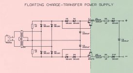
Floating CT power supply test
Hi all,
Today I tested the floating charge transfer power supply for the D1M. This one also interrupts GND, so the output voltage truly floats.
I attached the concept schematic diagram.
There is a rectifier bridge (D1 ... D4) using schottky diodes (11DQ10 will be ok too), creating a plus and minus voltage, charging C1 and C2 through D5 ... D8. These diodes are required to create pulsed DC signals for driving both darlingtons, and set the exact switching level. Both R1 and R2 are used to provide a base drive current for the darlington switches. The charge across C1 and C2 is transferred to C3. N1, N2, R3, R4, D9, and D10 are used to attenuate switching noise.
After powering up, magic was in the air 🙂
Attachments

- Home
- Source & Line
- Digital Line Level
- Building the ultimate NOS DAC using TDA1541A