connection cdpro2 to d1m
hi john,
if you do not recommend to connect the i2s output of the cdpro2 directly to the d1m, what would be the best way to do that? using directly the cdpro ebu/spdif output? (btw, this output does not require pulse transformer)
do you still consider a toslink for the new d1m?
how many modules does contain d1m in total ?
when do you think that your d1m modules are ready to sell; my birthday is coming very soon 🙂
kind regards
mamal
Dear ECdesigns,
Thanks for your previous answers and for the trans-impedance circuits; you are spoiling us!
Or maybe we are abusing of your kindness
They look simple enough to be understood by us, less gifted beings (he even draw arrows to make it easier)
About CD PRO, the idea is to use very short I2S wires with the DAC inside the transport box and one of two options; replace the transport's own system clock for a better one ( I assume BCK will be derived from it (?)) or re-clock BCK at the DAC board and slave the transport back, as you said...and don't know which one is worse! 😀 Anyway, I doubt it'll sound too bad...
Global warming is interesting to say the least; it is probable that the explanation is(are) a natural cycle(s) but it is appealing to blame our fellow men... 🙂 It increases our sense of virtuosity.
Cheers,
M
"Charge transfer addict"
Hi mr whocares,
The I2S signals are fine, and could be used when the DAC is placed in the same housing as the CDPROII, still the I2S signals would have to be synchronously reclocked with a low jitter masterclock, prior to feeding them to the DAC chip. Glue logic may be required to match the format used.
When using the external D1M DAC, I would tap the ebu/spdif signal from the CDPROII electronics, preferably TTL level. Next I would synchronously reclock this ebu/spdif signal with a low jitter masterclock that's also used to clock the CDPROII electronics. I would then feed this cleaned-up SPDIF signal to a Toslink optical transmitter.
I would use real glass-fibre Toslink interlinks, NOT the cheap ones with single clear plastic core. This reduces unwanted reflections.
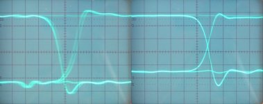
The D1M has a double SPDIF receiver front-end. The first SPDIF receiver cleans-up the Toslink signal after the Toslink optical receiver, the second performs the actual decoding. Both SPDIF receivers run in slave-clock mode. I attached an oscillogram illustrating SPDIF cleaner efficiency.
Left oscillogram shows a typical SPDIF signal (Toslink), using a cheap plastic interlink of 10 meters and a lousy Toslink digital audio source. On the right is the same signal after passing the SPDIF cleaner. When using shorter, high-quality, real glass-fibre interlinks, things will only get better.
The CDPROII has an on-board pulse transformer. Even the best pulse transformers have coupling capacitance between both primary and secondary windings (low enough impedance for HF interference to pass). The pulse transformer also has a large bandwidth, so all HF interference can travel together with the spdif signal into the connected DAC. This can be easily verified by observing the received SPDIF signal (phase) noise.
Toslink has limited bandwidth (approx. 10 MHz) this helps to reduce unwanted HF interference from reaching the DAC electronics. This bandwidth is more than sufficient to transport the SPDIF serial data (up to 96 KHz bit rate). 96 KHz bit rate requires approx. 6.144 MHz clock signal that's still within Toslink bandwidth.
The D1M already runs on Toslink. It can also accept USB, using an external USB to Toslink converter. This provides USB option with full galvanic insulation as well. It supports 44.1, 48, 88.2, and 96 KHz sample rates. Since the D1M has CS8416 SPDIF receivers (that can even be swapped with any other receiver because of the modular design), SPDIF coax could also be used.
4 Modules:
- SPDIF module #1, used as SPDIF cleaner, running in slave clock mode.
- SPDIF module #2, used as main SPDIF receiver running in slave clock mode.
- Multi-rate masterclock / tracker / buffer module.
- Stereo trans-impedance converter.
All other parts are mounted on the single 10 x 22 cm main board. The D1M is powered externally, using a plain mains adapter, charge-transfer power supply, or 12V battery power supply.
If you are in a hurry, I could manufacture some prototype PCBs (similar to the ones posted photographs), they are reliable enough to last for decades. It will take some time before I can order the professionally manufactured PCBs, as I want to combine many different PCBs on one panel in order to reduce cost.
if you do not recommend to connect the i2s output of the cdpro2 directly to the d1m, what would be the best way to do that? using directly the cdpro ebu/spdif output?
The I2S signals are fine, and could be used when the DAC is placed in the same housing as the CDPROII, still the I2S signals would have to be synchronously reclocked with a low jitter masterclock, prior to feeding them to the DAC chip. Glue logic may be required to match the format used.
When using the external D1M DAC, I would tap the ebu/spdif signal from the CDPROII electronics, preferably TTL level. Next I would synchronously reclock this ebu/spdif signal with a low jitter masterclock that's also used to clock the CDPROII electronics. I would then feed this cleaned-up SPDIF signal to a Toslink optical transmitter.
I would use real glass-fibre Toslink interlinks, NOT the cheap ones with single clear plastic core. This reduces unwanted reflections.
The D1M has a double SPDIF receiver front-end. The first SPDIF receiver cleans-up the Toslink signal after the Toslink optical receiver, the second performs the actual decoding. Both SPDIF receivers run in slave-clock mode. I attached an oscillogram illustrating SPDIF cleaner efficiency.
Left oscillogram shows a typical SPDIF signal (Toslink), using a cheap plastic interlink of 10 meters and a lousy Toslink digital audio source. On the right is the same signal after passing the SPDIF cleaner. When using shorter, high-quality, real glass-fibre interlinks, things will only get better.
(btw, this output does not require pulse transformer)
The CDPROII has an on-board pulse transformer. Even the best pulse transformers have coupling capacitance between both primary and secondary windings (low enough impedance for HF interference to pass). The pulse transformer also has a large bandwidth, so all HF interference can travel together with the spdif signal into the connected DAC. This can be easily verified by observing the received SPDIF signal (phase) noise.
Toslink has limited bandwidth (approx. 10 MHz) this helps to reduce unwanted HF interference from reaching the DAC electronics. This bandwidth is more than sufficient to transport the SPDIF serial data (up to 96 KHz bit rate). 96 KHz bit rate requires approx. 6.144 MHz clock signal that's still within Toslink bandwidth.
do you still consider a toslink for the new d1m?
The D1M already runs on Toslink. It can also accept USB, using an external USB to Toslink converter. This provides USB option with full galvanic insulation as well. It supports 44.1, 48, 88.2, and 96 KHz sample rates. Since the D1M has CS8416 SPDIF receivers (that can even be swapped with any other receiver because of the modular design), SPDIF coax could also be used.
how many modules does contain d1m in total ?
4 Modules:
- SPDIF module #1, used as SPDIF cleaner, running in slave clock mode.
- SPDIF module #2, used as main SPDIF receiver running in slave clock mode.
- Multi-rate masterclock / tracker / buffer module.
- Stereo trans-impedance converter.
All other parts are mounted on the single 10 x 22 cm main board. The D1M is powered externally, using a plain mains adapter, charge-transfer power supply, or 12V battery power supply.
when do you think that your d1m modules are ready to sell; my birthday is coming very soon
If you are in a hurry, I could manufacture some prototype PCBs (similar to the ones posted photographs), they are reliable enough to last for decades. It will take some time before I can order the professionally manufactured PCBs, as I want to combine many different PCBs on one panel in order to reduce cost.
Attachments
hi john,
thanks for your reply and the info. it seems that your project is being to come to really the final phase/version 🙂 and i am very interested to try your dac.
i will contact you regarding your offer.
have a nice weekend
cheers
mamal
thanks for your reply and the info. it seems that your project is being to come to really the final phase/version 🙂 and i am very interested to try your dac.
i will contact you regarding your offer.
have a nice weekend
cheers
mamal
Hi John,
Ever since I implemented the attenuation of WS and DATA I have experienced problems with my DAC.
I have tried lower resistor values and have now returned to 10ohm resistors which does not solve the problem.
I am using a sync reclocker with output from a Squeezebox 2. I can play 1-2 tracks before the output distorts, sounding a bit like an FM radio scanning, and then I either get hiss or a mid frequency hum. The problem clears when I remove the power from the squeezebox and restart.
This is really frustrating as the DAC sounds great with the reclocker.
Any ideas?
I am looking forward to buying your modules! - then, hopefully, I will cause less problems with my tweaking!
Brad
Hi Builder Brad,
I need some more information for solving this problem, if you could email schematics, I will have a look.
Some information about TDA154x digital inputs. The TDA154x chips use current steering and are based on bipolar transistors.
Each digital input has 3 diodes in series (approx. 3 x 0.6V = 1.8V) tied to a constant current source that goes to VCC or +5V. The input pin is connected to the junction of current source and anode of upper diode, through a 4th series diode. The anode of this series diode connects to the constant current source, the cathode connects to the digital input pin (TDA1543 datasheet page 5). The two additional diodes at the input pin are protection diodes.
The 3 diodes in series set the logic "1" level. So an input voltage below 1.8 - 0.6 = 1.2V, will be able to produce a logic "0". Voltage above 1.2V will prevent the input series diode from conducting, the constant current source will now set the logic "1" level of 1.8 Volts.
The resistive attenuators provide (1000 / (1000 + 3300)) * 5 = 1.16V threshold voltage, this voltage is optimized for a TDA154x that has reached normal operating temperature. Attenuator shunt resistance equals (1000 + 3300) / (3300 + 1000) = 767 Ohms. Attenuator series resistor equals 3300 Ohms. The resulting ac signal across the 1.16V reference voltage equals (767 / (3300 + 767)) * 5 = 0.943Vpp. Logic "0" level equals 1.16 - 0.471 = 0.69V, logic "1" level equals 1.16 + 0.471 = 1.631V.
I now use I2S attenuators in all my DACs, and they function perfectly up to 96 KHz sample rate, still using 3K3 series resistor, 1K to GND, and 3K3 to VCC. I even attenuated BCK, 330R series resistor, 330R to a low-noise VCC, and 100 Ohms to GND.
I have to add that I use short I2S interlinks (few centimeters max.). I also run the DAC chip(s) directly from the master clock, so there are no delays introduced by a (synchronous) reclocker.
Ever since I implemented the attenuation of WS and DATA I have experienced problems with my DAC.
I am using a sync reclocker with output from a Squeezebox 2. I can play 1-2 tracks before the output distorts, sounding a bit like an FM radio scanning, and then I either get hiss or a mid frequency hum. The problem clears when I remove the power from the squeezebox and restart.
I need some more information for solving this problem, if you could email schematics, I will have a look.
Some information about TDA154x digital inputs. The TDA154x chips use current steering and are based on bipolar transistors.
Each digital input has 3 diodes in series (approx. 3 x 0.6V = 1.8V) tied to a constant current source that goes to VCC or +5V. The input pin is connected to the junction of current source and anode of upper diode, through a 4th series diode. The anode of this series diode connects to the constant current source, the cathode connects to the digital input pin (TDA1543 datasheet page 5). The two additional diodes at the input pin are protection diodes.
The 3 diodes in series set the logic "1" level. So an input voltage below 1.8 - 0.6 = 1.2V, will be able to produce a logic "0". Voltage above 1.2V will prevent the input series diode from conducting, the constant current source will now set the logic "1" level of 1.8 Volts.
The resistive attenuators provide (1000 / (1000 + 3300)) * 5 = 1.16V threshold voltage, this voltage is optimized for a TDA154x that has reached normal operating temperature. Attenuator shunt resistance equals (1000 + 3300) / (3300 + 1000) = 767 Ohms. Attenuator series resistor equals 3300 Ohms. The resulting ac signal across the 1.16V reference voltage equals (767 / (3300 + 767)) * 5 = 0.943Vpp. Logic "0" level equals 1.16 - 0.471 = 0.69V, logic "1" level equals 1.16 + 0.471 = 1.631V.
I now use I2S attenuators in all my DACs, and they function perfectly up to 96 KHz sample rate, still using 3K3 series resistor, 1K to GND, and 3K3 to VCC. I even attenuated BCK, 330R series resistor, 330R to a low-noise VCC, and 100 Ohms to GND.
I have to add that I use short I2S interlinks (few centimeters max.). I also run the DAC chip(s) directly from the master clock, so there are no delays introduced by a (synchronous) reclocker.
I attached some basic trans-impedance circuits that could be used for further experiments. The D1M is running on a highly optimized version, based on similar techniques. Note that the DAC current sink runs straight through T1 (that's kept in saturation), and directly flows through the passive I/V resistor R1. So basically iDAC = iRiv. I have to add that the 12V supply must be as clean as possible. The low-noise bandgap reference is required to provide approx. 2.1V DC at the TDA1543 output (2.7V - 0.6V).
With regards to transimpedance amplifier for the tDA 1541a, can I use the diode let's say 1N4001 to replace the U1. Also I will replace Riv to 1K41. Assuming if I cant get 1k41, should I go lower or higher ?
Just wonder how by connecting a diode (replace U1) can give a Vref of 0.6 V ?
hi john,
i just sent you an email to ecdesigns. please let me know in case the mail did not arrive.
regards
mamal
i just sent you an email to ecdesigns. please let me know in case the mail did not arrive.
regards
mamal
Hi ccschua,
Use either a diode like 1N4148, or a 2SC2240 connected as diode.
In the schematic, U1, 1N4148 anode to plus of C1, 1N4148 cathode (black indication ring) to GND). In case of 2SC2240 used as matching diode, collector + basis to plus of C1, emitter to GND. This will create 0.6V voltage drop across the diode that's used for reference voltage.
I/V resistor (1K41), use closest match, like MRS25 series 1K4. When using 1K5, output voltage will be slightly increased to 0.004 x 1500 = 6Vpp or 2.12V rms.
Higher resistor value will give higher output voltage, too high output voltage may cause clipping when 12V power supply remains unchanged.
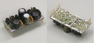
Back on topic, Today I manufactured and tested the final module for the new D1M, it's the stereo trans-impedance I/V converter / buffer module.
I attached a photograph of this module, on the left is the component side view. The electrolytics in the center are decoupling caps for the precision reference voltages. I/V resistors are modified 2K5 bulk metal foils from Vishay. The black bulk metal foil resistors, and the round chokes are part of the single-ended output buffer. The light brown Murata filters are used to stabilize precision correction current sources that prevent T1 (in the schematic) from going out of conduction and ensuring TDA1543 output compliance. Both T1 and T2 consist of 2 transistors in parallel in order to further reduce noise levels. The module is designed to run on a super-clean 9.2V power-shunt regulator. It connects directly to the TDA1543 outputs, and requires an Intertechnik 4.7uF polypropylene / TIN foil coupling cap on the output. This cap was chosen for very detailed, crystal clear trebles, and optimal transparency.
Photograph on the right shows the solder side, there are some SMD resistors and some reference diodes for the correction current sources. The gold-plated pins were pressed into the PCB using a special bench press, then soldered on both sides. The whole module (PCB included) was manufactured, assembled and tested within a few hours.
I received some questions about how the D1M compares to the DI4T. Well I seldom listen to the DI4T anymore, and only use it as reference when needed. The D1M prototype is almost used constantly, this should say enough.
The D1M was based on techniques and knowledge gathered over the past years. The aim was designing a cheaper miniature DAC that performs (almost) equal to the DI4T. It resulted in a miniature DAC outperforming and replacing the DI4T.
The D1M has a unique SPDIF reclocker, main SPDIF receiver and the new multi-rate masterclock tracker. The TDA1543 simply baffled me, never expected such performance was possible using a tiny 8-pin budget chip. Specs aren't that impressive either. Possible explanation is the simple straight-forward chip design with few on-chip interference sources.
The TDA1543 has I2S attenuators on all inputs and now runs on 4 volts. The TDA1543 current outputs drive a trans-impedance I/V converter / buffer.
Yesterday I designed new power supplies for the D1M, I removed all 78xx regulators.
The D1M power supplies were designed to run on "anything" providing approx. 12 ... 15 volts DC, including $3, 12V mains adapters and 12V lead-acid batteries.
There are two discrete, low-noise pre-regulators, one 5V and one 9.6V regulator. Both have integrated current limiter. The regulators are built around the TL431 voltage reference and require only few parts, no OP-amps were used.
Starting with the 5V pre-reg, it drives TDA1543, both SPDIF receivers, and some logic. Each of these circuits runs on a precision low-noise power-shunt, connected through a 10mH choke, power-shunt voltage is set at 4 volts. The power-shunts are based on a TL431, but have much lower impedance, and can handle high currents (up to approx. 5 amps).
The 9.6V pre-reg drives the trans-impedance converter through a 10mH choke, the trans-impedance converter runs on a 9.2V power-shunt.
The multi-rate masterclock / tracker module is fed through a high precision current source that's based on a TL431 voltage reference and a low-noise OP-amp. The current source connects to a low-pass filter (40mH and 100,000uF) and then feeds a 5V power-shunt.
Next task is to design a 10 x 22 cm mainboard for the D1M.
With regards to transimpedance amplifier for the tDA 1541a, can I use the diode let's say 1N4001 to replace the U1. Also I will replace Riv to 1K41. Assuming if I cant get 1k41, should I go lower or higher ?
Just wonder how by connecting a diode (replace U1) can give a Vref of 0.6 V ?
Use either a diode like 1N4148, or a 2SC2240 connected as diode.
In the schematic, U1, 1N4148 anode to plus of C1, 1N4148 cathode (black indication ring) to GND). In case of 2SC2240 used as matching diode, collector + basis to plus of C1, emitter to GND. This will create 0.6V voltage drop across the diode that's used for reference voltage.
I/V resistor (1K41), use closest match, like MRS25 series 1K4. When using 1K5, output voltage will be slightly increased to 0.004 x 1500 = 6Vpp or 2.12V rms.
Higher resistor value will give higher output voltage, too high output voltage may cause clipping when 12V power supply remains unchanged.
Back on topic, Today I manufactured and tested the final module for the new D1M, it's the stereo trans-impedance I/V converter / buffer module.
I attached a photograph of this module, on the left is the component side view. The electrolytics in the center are decoupling caps for the precision reference voltages. I/V resistors are modified 2K5 bulk metal foils from Vishay. The black bulk metal foil resistors, and the round chokes are part of the single-ended output buffer. The light brown Murata filters are used to stabilize precision correction current sources that prevent T1 (in the schematic) from going out of conduction and ensuring TDA1543 output compliance. Both T1 and T2 consist of 2 transistors in parallel in order to further reduce noise levels. The module is designed to run on a super-clean 9.2V power-shunt regulator. It connects directly to the TDA1543 outputs, and requires an Intertechnik 4.7uF polypropylene / TIN foil coupling cap on the output. This cap was chosen for very detailed, crystal clear trebles, and optimal transparency.
Photograph on the right shows the solder side, there are some SMD resistors and some reference diodes for the correction current sources. The gold-plated pins were pressed into the PCB using a special bench press, then soldered on both sides. The whole module (PCB included) was manufactured, assembled and tested within a few hours.
I received some questions about how the D1M compares to the DI4T. Well I seldom listen to the DI4T anymore, and only use it as reference when needed. The D1M prototype is almost used constantly, this should say enough.
The D1M was based on techniques and knowledge gathered over the past years. The aim was designing a cheaper miniature DAC that performs (almost) equal to the DI4T. It resulted in a miniature DAC outperforming and replacing the DI4T.
The D1M has a unique SPDIF reclocker, main SPDIF receiver and the new multi-rate masterclock tracker. The TDA1543 simply baffled me, never expected such performance was possible using a tiny 8-pin budget chip. Specs aren't that impressive either. Possible explanation is the simple straight-forward chip design with few on-chip interference sources.
The TDA1543 has I2S attenuators on all inputs and now runs on 4 volts. The TDA1543 current outputs drive a trans-impedance I/V converter / buffer.
Yesterday I designed new power supplies for the D1M, I removed all 78xx regulators.
The D1M power supplies were designed to run on "anything" providing approx. 12 ... 15 volts DC, including $3, 12V mains adapters and 12V lead-acid batteries.
There are two discrete, low-noise pre-regulators, one 5V and one 9.6V regulator. Both have integrated current limiter. The regulators are built around the TL431 voltage reference and require only few parts, no OP-amps were used.
Starting with the 5V pre-reg, it drives TDA1543, both SPDIF receivers, and some logic. Each of these circuits runs on a precision low-noise power-shunt, connected through a 10mH choke, power-shunt voltage is set at 4 volts. The power-shunts are based on a TL431, but have much lower impedance, and can handle high currents (up to approx. 5 amps).
The 9.6V pre-reg drives the trans-impedance converter through a 10mH choke, the trans-impedance converter runs on a 9.2V power-shunt.
The multi-rate masterclock / tracker module is fed through a high precision current source that's based on a TL431 voltage reference and a low-noise OP-amp. The current source connects to a low-pass filter (40mH and 100,000uF) and then feeds a 5V power-shunt.
Next task is to design a 10 x 22 cm mainboard for the D1M.
Attachments
continued
Would it be asking too much to see these TL431 based reg ccts? The TooleShunt Reg is not so simple now, and your designs appear small enough to use everywhere.
Would it be asking too much to see these TL431 based reg ccts? The TooleShunt Reg is not so simple now, and your designs appear small enough to use everywhere.
Hi jameshillj,
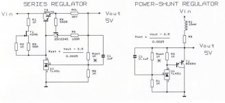
No, of course not, I attached a schematic diagrams of both discrete series regulator and power shunt.
The series regulator is based on a TL431 voltage reference. RCL, R4, R5 and T3 are an optional current limiter. If no current limiting is required, RCL is bypassed and T3, R4, and R5 can be left-out. Voltage is set with Rset, circuit shows a 5V regulator. For 12V output for example, Rset would need to be (12 - 2.5) / 0.0025 = 3800 Ohms. The constant current source around T1 feeds the voltage reference, it could be replaced by a resistor, but then performance would drop.
The power shunt on the right is basically a buffered TL431 shunt regulator, BC684 can handle up to approx. 4 amps, it needs to be mounted on a suitable heatsink when using larger bias currents. I added a choke (optional) in series with the power-shunt for attenuating power supply noise.
Would it be asking too much to see these TL431 based reg ccts? The TooleShunt Reg is not so simple now, and your designs appear small enough to use everywhere.
No, of course not, I attached a schematic diagrams of both discrete series regulator and power shunt.
The series regulator is based on a TL431 voltage reference. RCL, R4, R5 and T3 are an optional current limiter. If no current limiting is required, RCL is bypassed and T3, R4, and R5 can be left-out. Voltage is set with Rset, circuit shows a 5V regulator. For 12V output for example, Rset would need to be (12 - 2.5) / 0.0025 = 3800 Ohms. The constant current source around T1 feeds the voltage reference, it could be replaced by a resistor, but then performance would drop.
The power shunt on the right is basically a buffered TL431 shunt regulator, BC684 can handle up to approx. 4 amps, it needs to be mounted on a suitable heatsink when using larger bias currents. I added a choke (optional) in series with the power-shunt for attenuating power supply noise.
Attachments
Regs
Thanks John for the ccts and the info.
Fascinating, and so simple, particularly in comparison to the developing Toole shunt Reg.
Could I further ask - how would you go about inverting these for the -ve voltages for the 1541A, the Kwak clock and my present Rudolf I/V output stages (+/- 18V)?
And, on your previous post, you mentioned that the 1543 chip is fed directly from the master clock at the 11.28Meg w/out reduction to reduce buffer and divider jitter, if I got that right - does the same apply to the 1541A chip (both NOS, naturally)?
Many thanks , and looking forward to the continuing developments of those amazing original dac chips.
Hi Luxury54,
how's your TDA1541A doing ? hav u reclock the DEM and did u put in a tube IV ?
What is the tantulum bypass value u use and brand ? is kemet ok ?
how's your TDA1541A doing ? hav u reclock the DEM and did u put in a tube IV ?
What is the tantulum bypass value u use and brand ? is kemet ok ?
Hi ccschua,
i finally have put together the DAC KIT from the small pieces and i have added a tube SRPP stage after resistor I/V conversion this way jumping the whole analog stage and enjoying a natural analog like tube sound with it's specific warm midrange ,very crisp highs and very good dynamics due to tube's high slew rate
i don't look any further for improvements just a DEM Reclocking and i'm going to "house" the kit in a fancy aluminium external CD-Rom enclosure
Here are some pictures in the process 😀
An externally hosted image should be here but it was not working when we last tested it.
An externally hosted image should be here but it was not working when we last tested it.
An externally hosted image should be here but it was not working when we last tested it.
An externally hosted image should be here but it was not working when we last tested it.
An externally hosted image should be here but it was not working when we last tested it.
An externally hosted image should be here but it was not working when we last tested it.
An externally hosted image should be here but it was not working when we last tested it.
An externally hosted image should be here but it was not working when we last tested it.
An externally hosted image should be here but it was not working when we last tested it.
An externally hosted image should be here but it was not working when we last tested it.
An externally hosted image should be here but it was not working when we last tested it.
An externally hosted image should be here but it was not working when we last tested it.
An externally hosted image should be here but it was not working when we last tested it.
An externally hosted image should be here but it was not working when we last tested it.
Hi Luxury,
Looks like your unit has better packaging than mine. I dont even have a manual.
Do try out the DEM reclocking. It certainly improve the sound. I wonder what IV resistor u use for tube SRPP ? Is there a finished kit on tube output ?
Looks like your unit has better packaging than mine. I dont even have a manual.
Do try out the DEM reclocking. It certainly improve the sound. I wonder what IV resistor u use for tube SRPP ? Is there a finished kit on tube output ?
ccschua said:Hi Luxury,
Looks like your unit has better packaging than mine. I dont even have a manual.
Do try out the DEM reclocking. It certainly improve the sound. I wonder what IV resistor u use for tube SRPP ? Is there a finished kit on tube output ?
the I/V resistor is Vishay 100 ohm metal foil (anything between 90-100 would do the job) which is directly from the tube's grid to ground as the TDA's outputs are tied to the grids of both tubes
used 6N2P in SRPP topology with 200 ohm cathode to ground and output cap a 2,2 uF Mundorf "M-Cap Audiophiler"
150V anode voltage and 6,3V (350 mAH) fillament voltage
An externally hosted image should be here but it was not working when we last tested it.
An externally hosted image should be here but it was not working when we last tested it.

Hi zoran,
I hate to admit it, since I used to be so pleased with tube sound quality, but the latest trans-impedance I/V converter module easily outperforms highly-tuned tube-based I/V converters by a VERY large margin.
- Distortion (THD) is way lower.
- Virtually zero phase errors (large bandwidth / high stability).
- The sound is highly transparent, and tonal balance is virtually perfect.
- Noise / interference is way lower.
It's also very difficult to find a "good sounding" tube. They are either to harsh (grainy) or too laid-back and midrange-forward. There is also a big quality difference between plain tubes and factory selected matched / balanced tubes. ECC82 isn't the best choice either, there are better tubes, but availability could get problematic. Some of the best tubes are out of production and are becoming very rare / expensive. When using a tube output, it's best to use a trans-impedance circuit like Guido Tent did (CD player kit).
Yesterday I tested Vcap (teflon and tin) coupling caps with the D1M (special thanks goes to erikdebest). D1M sound quality really excelled, leaving me completely stunned, it's a HUGE difference. The 2K5 passive I/V resistor is a modified Vishay S102J bulk metal foil resistor.
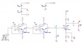
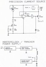
TDA1543 is now running at 3.1 volts, and I2S signal levels (including BCK) were lowered to approx. 400mVpp. The modified shunt, driving the TDA1543 and I2S attenuators has approx. 0.05 Ohm impedance now. The master clock tracker power supply uses a precision constant current source, connected to a discrete 9.6 volt series pre-regulator. The precision current source drives the power shunt (0.025 Ohm impedance) through passive LC filters. I attached a schematic diagram of the precision current source, and the block diagram of the master clock power supply.
Yesterday I also completed a new charge transfer power supply, it has both plus and minus interrupted (dual charge-transfer circuits). I plan to test it with the D1M.
Someone asked for iv with ecc82...
I hate to admit it, since I used to be so pleased with tube sound quality, but the latest trans-impedance I/V converter module easily outperforms highly-tuned tube-based I/V converters by a VERY large margin.
- Distortion (THD) is way lower.
- Virtually zero phase errors (large bandwidth / high stability).
- The sound is highly transparent, and tonal balance is virtually perfect.
- Noise / interference is way lower.
It's also very difficult to find a "good sounding" tube. They are either to harsh (grainy) or too laid-back and midrange-forward. There is also a big quality difference between plain tubes and factory selected matched / balanced tubes. ECC82 isn't the best choice either, there are better tubes, but availability could get problematic. Some of the best tubes are out of production and are becoming very rare / expensive. When using a tube output, it's best to use a trans-impedance circuit like Guido Tent did (CD player kit).
Yesterday I tested Vcap (teflon and tin) coupling caps with the D1M (special thanks goes to erikdebest). D1M sound quality really excelled, leaving me completely stunned, it's a HUGE difference. The 2K5 passive I/V resistor is a modified Vishay S102J bulk metal foil resistor.
TDA1543 is now running at 3.1 volts, and I2S signal levels (including BCK) were lowered to approx. 400mVpp. The modified shunt, driving the TDA1543 and I2S attenuators has approx. 0.05 Ohm impedance now. The master clock tracker power supply uses a precision constant current source, connected to a discrete 9.6 volt series pre-regulator. The precision current source drives the power shunt (0.025 Ohm impedance) through passive LC filters. I attached a schematic diagram of the precision current source, and the block diagram of the master clock power supply.
Yesterday I also completed a new charge transfer power supply, it has both plus and minus interrupted (dual charge-transfer circuits). I plan to test it with the D1M.
Attachments
Hi ecdesigns,
a silly question regarding the i/v circuits in post 2540:
"Vref Other Channel" is only for the other channel of the stereo couple or also for Vref on 1543?
If not how do you manage Vref on 1543 in this implementation?
Thanks
Andrea
a silly question regarding the i/v circuits in post 2540:
"Vref Other Channel" is only for the other channel of the stereo couple or also for Vref on 1543?
If not how do you manage Vref on 1543 in this implementation?
Thanks
Andrea
- Home
- Source & Line
- Digital Line Level
- Building the ultimate NOS DAC using TDA1541A