About voltage offset (positive mV in the OUT pin), for me it appears "for free" when I injected the 2mA compensation current since I'm using a passive solution, and part of the load is pure R, and remaining is the cathode input impedance (AC coupled). Resulted in some +50mV offset.
Yes Diybras but this was in context of using USB me just wondering if it would be different for just Redbook playback
Is basically the same. The RC smoothing is for reducing the dV/dT at TDA inputs. Logic circuits produces it (fast risetime). Only changes a little the ideal values for 3V3 logic vs 5V logic (present in CD players). You can make the R value a little higher for 5V logic. Unless it is authentic TTL, then you can use same values as 3V3 CMOS logic.
I tried the attenuator/signal conditioner circuit in this article:
https://www.mvaudiolabs.com/digital/tda1541-digital-input-attenuation/
It works well.
https://www.mvaudiolabs.com/digital/tda1541-digital-input-attenuation/
It works well.

If I may, I recalled yrs back reading about using 100 ohm resistors on the I2S lines to slow or damped
the signals. Do they have any positive effects on SQ ?
Depends.
For TDA1541(A) we have a significant problem. The technology of the time (no 3nm finfet's back then) meant the input buffer PNP transistors are made in a way that means each input has a significant capacitance into the substrate, so fast edges from the clocks and data couple into the substrate and contaminate the output. There are secondary mechanisms that also contaminate the +5V/-5V rails with these same signal.
When using "attenuators" and "slew rate limiters" we minimise these effects. For example, limiting the bandwidth on the inputs (12pF capacitance) to ~ 10MHz (~ 16nS time constant) the coupling of BCK, WCH and Data into the substrate is much reduced. For 12pF and 16nS slew rate limit this suggest a 1.3k resistor in series with the signals AT THE TDA1541 Pin's.
If in addition to a 10MHz/16nS lowpass we can limit signal swing from ~ 0.9V to 1.8V this is an added bonus. But it is the lowpass that is important.
Of course, some will say that as long as you use stopped clock and and a jittery free running 50Hz oscillator with 100uF electrolytic capacitors non of this matters and it's all perfect sound forever.
For more modern IC's, every PCB trace is also an inductance (and capacitance - but inductance dominates). A 10mil wide 30mm long trace ideally is ~ 33nH, the typical input capacitance of a CMOS IC is 4.5pf. This forms an ~ 400MHz lowpass with an ~ 60dB peak at 400MHz. That trace will at every clock or data edge ring at ~400MHzwith a very high Q. A normal 100MHz 'scope may not even show much. Adding a 100R "damping" resistor at the beginning of the trace removes the peak. Making the resistor 330 Ohm kills the resonance completely and crates a 100MHz lowpass.
Does this help sound quality? Who knows. But any output that produces high dV/dT edges should have a series resistor, ideally optimised for the desired waveform (active < 1pF 'scope probe @ >> 100MHz bandwidth for Audio), which can lead to surprisingly high values. It is better for EMC and EMI for sure.
Thor
Hi studiostevus,Interesting explanation, would a differential dac setup neutralize the glitch, assuming 'matched' TDA's? or is the likelihood of catching the spike timing just right near impossible, which I understand is one of the problems in the complex Nakamichi patent solution.
As far as im aware the Signed Magnitude approach eliminates this glitch but I haven't heard of anyone getting it to work correctly though.
TDA1541A Dual Mono 17 bit Signed Magnitude DAC
With conventional (R2R / multibit) D/A converters all bits flip over simultaneously at the signal zero crossing. This produces both, switching noise and bit errors.
Our auditory system seems to be highly sensitive to everything that happens around these zero crossings. Now you know why class A amplifiers make a lot of sense as these will reduce but never fix problems around zero crossings and why SE amplifiers -can- sound so musical and involving as these reproduce zero crossings so accurately like no other amp can. The speakers are no exception either, problems, problems.
But lets concentrate on the DAC first. What could cause problems around zero crossings? all bits flipping over at the same time, just at most critical point in the audio signal.
1000000000000000 -> 0111111111111111, we have 16 bits flipping over simultaneously around the zero crossing!
This problem can be fixed if we use a signed magnitude DAC. As the name implies we have a sign bit (positive or negative) indicating the polarity and magnitude information (number) that, well determines the signal magnitude.
And what's so different about this approach?
With signed magnitude we usually have two identical DACs. One handles the positive signal halve only, the other handles the negative signal half only.
Now we can step away from the zero crossing with small steps in both directions like this:
Signal rises from zero crossing to plus, 000000000000000 -> 000000000000001 -> 000000000000010 and so on. L channel never goes below 000000000000000, we have only one bit flipping around the signal crossover, positive DAC is working, negative DAC takes a break.
Signal drops from zero crossing to minus, 111111111111111 -> 111111111111110 -> 111111111111101 and so on. R channel never goes above 111111111111111, we have only one bit flipping around the signal crossover. negative DAC is working, positive DAC takes a break.
MSB now becomes the sign bit that controls the polarity and no longer shows up in the data (magnitude) of both DACs. So we have a spare (extra) bit where MSB used to be. Now we can also double the resolution.
The outputs of both DACs are connected together.
Some examples of signed magnitude D/A converters are the Soekris DAC and the PCM1704 just to name a few of many.
The TDA1541A has two identical DACs that are usually used for L and R channel. But what if we used both channels to construct a signed magnitude mono DAC with it? We would need two TDA1541A chips as we need 4 DACs in total now. We end up with a 17 bit dual mono TDA1541A signed magnitude DAC, full scale current doubles to 8mA and resolution is doubled to 17 bits. Now this would be a very nice project for two (double crown) TDA1541A chips.
All we need to do is design a decoder that moves some bits around so we end up with output signals DOL- and DOL+ for TDA1541A #1 and DOR- and DOR+ for TDA1541A #2.
We could use a FPGA or ASIC, however, the nasty thing here is that we need to reduce (switching) noise to lowest practical level and that's going to be extremely difficult with these LSI chips that produce very strong interference. Even a tiny PAL (Programmable Array Logic) produces massive switching noise and draws a lot of current.
So there is little other option then building a decoder from a handful of discrete logic so we only use and connect those logic building blocks we need and we can locally decouple all these logic building blocks until switching noise is as low as it gets. Current consumption is also absolute minimum this way.
IF we insist using a noisy ASIC or CPU we have to ensure that the D/A converter is -completely- shielded (EMI included) from this switching noise, I wish you good luck with that.
Back to the Decoder circuit. I attached a schematic of a decoder I designed for this experiment, it is based on the protocol converter I posted earlier. It looks complicated but it is basically as simple as it gets.
We need to do a few things, sample and hold the MSBs, then loose the LSBs from the serial data that goes into the TDA1541A chips. Mix MSB and data signals together so we get dedicated data signals for each TDA1541A.
We know that the MSB are located immediately after a WS change (I use Left justified format!). So we need to create a trigger signal right at the center of these MSBs. We need 0.5 bit delay for that and that's provided by U1. We need to keep the Left MSB with the Left data and the Right MSB with the right data. So we have to invert the 0.5 bit delay signal for one channel. U4 and U5 sample and hold the MSB for each channel, we use these sampled MSBs in the decoder stage.
Loose the MSB, easier said then done as we can't easily shift the serial data to the left unless we add some more shift registers.
Instead I delayed the window that determines when the output signals are generated in relation to WS. By delaying the window signal by one bit I basically removed the MSBs from the serial bit stream, after I have sampled the MSBs of course.
The output of U2 provides a 1 bit delay and the delayed signal goes to the window generator built around counter U6 and NOR gate U17.
U3 lines up the left channel data so the bits are valid on the falling edge of BCKI (TDA1541A clocks on the falling edge of BCK when configured in the simultaneous mode).
U7 ... U10 line up the Right channel data with the Left channel data so both can be clocked out simultaneously.
U16 gates the bit clock so we have a 16 bit clock burst at just the right time. The window signal enables and disables the continuous BCKI signal.
U13 B and D do the same for the serial data, creating 16 bit data bursts at just the right moment.
U13A, U14, U13C and U15 form a simple AND / OR decoder that extracts DOL-, DOL+, DOR-, and DOR+ signals from the serial data streams.
People who need to have I2S input will have to add some more logic as MSB is shifted one bit to the right (with respect to WS) and both channels are swapped.
What we have to do now is adding one extra D flip-flops to sample the MSBs one and a half bit after a WS change (1.5 bit delay) and a 2 bit delay to drive the window generator so we still loose the MSB. DOL becomes DOR and DOR becomes DOL (swap channels) and we are ready to use I2S input signal.
Second picture shows the timing diagram. We can see that the whole window is shifted one bit to the right compared to the protocol converter timing diagram.
Third schematic shows the TDA1541A section. We need +4mA bias current for biasing two converters. This can be done using a 1K1 resistor between outputs and +5V. I try to avoid a CCS whenever possible as these are -very- nasty circuits that often result in grainy fatiguing sound. I traced this back to the non-linear impedance that varies with frequency, adding a shunt resistor across the CCS can improve things a bit by linearising the impedance.
The simple CCS we see in many schematics are not very precise and for this application we need a high precision CCS with very large bandwidth and superb impedance linearity. This usually translates to complex analogue circuits that in turn introduce new problems.
The full scale current has doubled to 8mA so the passive I/V resistor value has to be reduced to 75 Ohms. We get approx. 560mVpp output (1K1 is in parallel with 75R for ac). This lower output impedance comes in handy when we like to drive a step up transformer or a TVC with a gain tap.
What conclusion do you draw from this?but I haven't heard of anyone getting it to work correctly though.
There is not much to see on the FFT. The 3rd HD increased a bit. However (or rather because of) the bit step accuracy is worse at 768 kHz DEM frequency, compared to 384 kHz. And THD is a little bit better at 384 kHz, compared to 192 kHz.Excellent. I'd be curious to see the FFT, but don't go out of your way,
Thor
Attachments

As far as im aware the Signed Magnitude approach eliminates this glitch but I haven't heard of anyone getting it to work correctly though.
Nope, I don't think so, because the Glitch for sign magnitude designs is generated by different mechanisms.
Thor
There is not much to see on the FFT. The 3rd HD increased a bit. However (or rather because of) the bit step accuracy is worse at 768 kHz DEM frequency, compared to 384 kHz. And THD is a little bit better at 384 kHz, compared to 192 kHz.
Interesting, at 768kHz we seem to get a "double glitch".
Thor
I can see what your alluding to but I dont think I can come to a conclusion based off someone else's experience without knowing what they concluded. I'd be interested in hearing from @koldby and what he ended up concluding from his experience from trying Ecdesigns signed magnitude approach.What conclusion do you draw from this?
That may explain the results koldby was getting. So in trying to solve one issue, another has been created.Nope, I don't think so, because the Glitch for sign magnitude designs is generated by different mechanisms.
Thor
It is actually a triggering issue on the oscilloscope. My fault.Interesting, at 768kHz we seem to get a "double glitch".
Thor
Hey @rfbrw, long time no see.What conclusion . . . . ?
Good to see some of the old folks from back when this thread started.
It is actually a triggering issue on the oscilloscope. My fault.
Ahh, ok. So no real visible changes, except more low level HD...
Thor
Even not having fast scope, good sense says to use these "slowing" rise rate resistors, and you have a excellente detailed explanation here, thanks (inclusing the CMOS case). (Besides long trace characteristic impedance in long tracks in multilayer PCB, for Z matching - I read about this but is beyond my DIY "free time").Depends.
For TDA1541(A) we have a significant problem. The technology of the time (no 3nm finfet's back then) meant the input buffer PNP transistors are made in a way that means each input has a significant capacitance into the substrate, so fast edges from the clocks and data couple into the substrate and contaminate the output. There are secondary mechanisms that also contaminate the +5V/-5V rails with these same signal.
When using "attenuators" and "slew rate limiters" we minimise these effects. For example, limiting the bandwidth on the inputs (12pF capacitance) to ~ 10MHz (~ 16nS time constant) the coupling of BCK, WCH and Data into the substrate is much reduced. For 12pF and 16nS slew rate limit this suggest a 1.3k resistor in series with the signals AT THE TDA1541 Pin's.
If in addition to a 10MHz/16nS lowpass we can limit signal swing from ~ 0.9V to 1.8V this is an added bonus. But it is the lowpass that is important.
Of course, some will say that as long as you use stopped clock and and a jittery free running 50Hz oscillator with 100uF electrolytic capacitors non of this matters and it's all perfect sound forever.
For more modern IC's, every PCB trace is also an inductance (and capacitance - but inductance dominates). A 10mil wide 30mm long trace ideally is ~ 33nH, the typical input capacitance of a CMOS IC is 4.5pf. This forms an ~ 400MHz lowpass with an ~ 60dB peak at 400MHz. That trace will at every clock or data edge ring at ~400MHzwith a very high Q. A normal 100MHz 'scope may not even show much. Adding a 100R "damping" resistor at the beginning of the trace removes the peak. Making the resistor 330 Ohm kills the resonance completely and crates a 100MHz lowpass.
Does this help sound quality? Who knows. But any output that produces high dV/dT edges should have a series resistor, ideally optimised for the desired waveform (active < 1pF 'scope probe @ >> 100MHz bandwidth for Audio), which can lead to surprisingly high values. It is better for EMC and EMI for sure.
Thor
I always loved to use such resistors even not having how to measure the benefits.
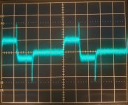
Now, for some "fun" 😉 / measurements, about my not ultimate TDA DAC (yet...)
The one from photos a lot of posts ago. Using yet the async DEM clock (no time yet to make the MCLK divider):
The J-Test generated by ARTA. For this case, I have 3 limitations:
1 - I cannot use the same PC as a generator and measuring device, due to ground loops. I not wanted to use coupling trafo this time. So, I generated the test in a notebook, and a PC having a Xonar audio board reads the result. SO the wave are not in sync;
2 - The notebook generating signal not have ASIO drivers, so maybe the WDM audio driver PERHAPS pollute the signal a little;
3 - the end limit is the Xonar ADC jitter.
Anyway:
Here a J-Test from the TDA1541 out, pusing the tube output stage:

And here is only the 12kHz signal:

Not too shabby for a collection of parts lying in drawers... 😀
The one from photos a lot of posts ago. Using yet the async DEM clock (no time yet to make the MCLK divider):
The J-Test generated by ARTA. For this case, I have 3 limitations:
1 - I cannot use the same PC as a generator and measuring device, due to ground loops. I not wanted to use coupling trafo this time. So, I generated the test in a notebook, and a PC having a Xonar audio board reads the result. SO the wave are not in sync;
2 - The notebook generating signal not have ASIO drivers, so maybe the WDM audio driver PERHAPS pollute the signal a little;
3 - the end limit is the Xonar ADC jitter.
Anyway:
Here a J-Test from the TDA1541 out, pusing the tube output stage:
And here is only the 12kHz signal:
Not too shabby for a collection of parts lying in drawers... 😀
Besides long trace characteristic impedance in long tracks
Let's be realistic.
The speed of an electric signal propagating as EM wave around the trace in a strip-line will be around 2/3C or 200,000km/S.
The highest speed edge in audio gear is likely is a 1nS rise time (that's VERY FAST logic).
A 10" long 50 Ohm PCB Strip line will produce around 1.25nS delay, thus a roundtrip with 0Ohm source and open end, will take 2.5nS, so clearly our edge gets distorted at both ends with minimal losses and rings across the line multiple times. That doubleplusungood for sure.
With a 12mil wide trace and 0.2mm dielectric thickness, we have 38.5pF capacitance. If we use 50 Ohm driving impedance, we have a 2nS time constant and thus a 80MHz lowpass where the rise time is limited to around 3nS. This means the much vaunted "transmission line" never happens.
We are dealing with an RLC lowpass that is damped. There is a good chance increasing the series resistor and thus setting lowpass to not allow the signals across trace to be faster than needed by the circuit will improve things further.
I would suggest that in most digital gear we work in audio there are no magical transmission lines (just more magical thinking), only more or less well damped LC resonance circuits, the damping of which may be adjusted by adding (material) resistance.
You need to get into 100's of MHz to have rather short traces to become a transmission line type problem.
There is still a benefit use matched impedance's, the damping is build in and predictable. But there is no reason to be excessively religious about it.
The same thing for trace length. Usually the quantity equalised by meandering traces is capacitance, not delay itself, delay equalisation is side effect of equalising capacitance.
Of course, if we design PC motherboards with PCIe 2X lanes, 5.6GHz DDR5 RAM etc. we are playing a different ballgame.
In a DAC, preferably keep all clocks as low frequency as will answer the requirements to pass signals. And keep the edge rate under control. And critically evaluate if faster edges REALLY reduce trigger uncertainty in a way that reduces jitter in the specific context.
Make sure edges are no faster than they need to be. Keeping "fast" signal traces short at the expense of "slow" traces is also a preferred compromise,
If the short trace has too little capacitance and edges are too fast, increase resistance to slow them down.
Thor
Last edited:
- Home
- Source & Line
- Digital Line Level
- Building the ultimate NOS DAC using TDA1541A