Excellent explanation, testemony to knowledge gained through hands-on experience, not just reading books or surfing forums.. . . . every PCB trace is also an inductance. A 10mil wide 30mm long trace ideally is ~ 33nH, the typical input capacitance of a CMOS IC is 4.5pf.
This forms an ~ 400MHz lowpass. That trace will at every clock or data edge ring at ~400MHzwith a very high Q. A normal 100MHz 'scope may not even show much. Adding a 100R "damping" resistor at the beginning of the trace removes the peak. Making the resistor 330 Ohm kills the resonance completely and crates a 100MHz lowpass.

Hi guys! I'm interested in this nos dac. Any idea when it will be available without any issues? Do I have to join a group buy or something to get on the list? Thanks!
when it will be available without any issues?
Probably never.
Do I have to join a group buy or something to get on the list?
There is no list.
You will have to use the knowledge exposed here to make your own DAC, I mean MAKE (not buy).
Thor
@ThorstenL Oh, I see. My mistake. Thanks for the info! I was under the impression that I could order various components and such and build my own. Have a nice day! 🙂
I was under the impression that I could order various components and such and build my own.
You can. You start by designing and making your own PCB or using Veroboard.
Thor
@ThorstenL Is it possible to have someone assemble the small smd components for me at a fee? I can solder the larger components, just not set up to do micro-soldering..lol
I am really enjoying the music I am listening to after building Gabi's TD1 DAC using a TDA1541A (https://www.youtube.com/playlist?list=PL2oZCBUlpvT8earHhMl3yjvMVzPtm-bw-)@ThorstenL Oh, I see. My mistake. Thanks for the info! I was under the impression that I could order various components and such and build my own. Have a nice day! 🙂
This playlist offers an easy-to-follow build sequence, which you can adapt to suit your abilities/preferences/wallet. I found Gabi extremely helpful - he resolved any problems I encountered in quick and courteous style, and I couldn't be happier with the end result 🙂
Gabster is a nicely thought out Stevie, if one is to build & just listen than its all fine but if one wants to get the best out of the TDA you just have to keep on experimenting & to discover as what Thorsten is trying to help us learn more.
Have a listen to this & you'll understand
https://www.facebook.com/share/v/19VSujoSwV/
Cheers
Have a listen to this & you'll understand
https://www.facebook.com/share/v/19VSujoSwV/
Cheers
@ThorstenL Is it possible to have someone assemble the small smd components for me at a fee? I can solder the larger components, just not set up to do micro-soldering..lol
My original idea was a project where we here design, make/test and then open-source a set of PCB designs that can be directly handled by a chinese PCB/PCBA house like JLCPCB.
We had a lot of good inputs that I think overall could make for an exceptional result.
If the group here had pooled their time and resources this could have happened, but it seems there was no interest in such a project and I don't have the time or inclination to do it single handed.
Thor
Latest prot. is done by the end of the year at least in my kitchen. Will test it out before releasing gerbers.
The Nakamichi patented glitch balance was tested with a 1 LSB step 1 kHz square signal. Ideally, the square signal has only odd harmonics. The even harmonics, 2 kHz, 4 kHz, etc. was cancelled by applying 40 ... 60 mV DC bias on the + input of the I/V opamp. Unfortunately the L and R channel needs different voltage: L = 54.1 mV, R = 38.2 mV on my specimen. (If a 10R resistor is inserted between AOL/AOR and the - input of the opamp, the idle -2 mA elevates this voltage by another 20 mV).
Attachments
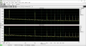
The Nakamichi patented glitch balance was tested with a 1 LSB step 1 kHz square signal. Ideally, the square signal has only odd harmonics. The even harmonics, 2 kHz, 4 kHz, etc. was cancelled by applying 40 ... 60 mV DC bias on the + input of the I/V opamp. Unfortunately the L and R channel needs different voltage: L = 54.1 mV, R = 38.2 mV on my specimen. (If a 10R resistor is inserted between AOL/AOR and the - input of the opamp, the idle -2 mA elevates this voltage by another 20 mV).
This looks excellent! This is no dither? Just direct +/-1LSB (so the raw performance baseline of 16 Bit?).
H3 at appx. -10dB from +/-1LSB is great. Just Curious what both channels look like with 46mV on both channels.
The addition of 10R with 10nA to ground before the resistor, any changes to wideband noisefloor with -60dBFS?
Thor
This is 0/1 LSB square wave, not sine, 24x 0's, 24x 1's with 48 kHz BCK. I think 1 LSB is -96 dBFS.
The addition of 10R with 10nF to ground before the resistor, any changes to wideband noisefloor with -60dBFS?
I could not detect any increase of noise floor, but my sound card is not very good, either.
The addition of 10R with 10nF to ground before the resistor, any changes to wideband noisefloor with -60dBFS?
I could not detect any increase of noise floor, but my sound card is not very good, either.
Hi! I would like to obtain the best DEM clock for my TDA1541 DAC in SIM mode get from CPLD by Miro code.352.8 KHz DEM clock schematics
Hi all,
I mentioned the new 352.8 KHz DEM clock circuit a number of times now,
Here it is, I attached a diagram of the 352.8 KHz DEM clock I currently use.
Depending on BCK frequency, BCK needs to be divided by a specific factor in order to get 352.8 KHz. When BCK equals 2.8224 MHz, a divide by 8 counter is needed, with other BCK frequencies the division factor needs to be adapted.
2.1168 MHz > divide by 6
2.8224 MHz > divide by 8
4.2336 MHz > divide by 12
5.6448 MHz > divide by 16
11.2896 MHz > divide by 32
Division factors like 6 and 12 can be obtained by resetting the synchronous counter, depending on a specific counter output code. Division factors like 32 can be obtained by cascading synchronous counters. This is achieved by connecting the clock inputs (pin 2) together, and connecting the TC output of the first counter (pin 15) to both CEP (pin 7) and CET (pin 10) of the second one.
When using a synchronous counter with asynchronous reset like the 74HC161, a divide by twelve counter can be constructed by resetting the counter at output code 1100 (12). This will produce an asymetrical output signal. To correct this a divide by 6 counter can be constructed (reset code 0110), followed by a synchronous divide by 2 counter.
When using synchronous counters with synchronous reset like 74HC163, the same divide by 12 counter can be constructed by resetting the counter at output code 1011 (11) as the synchronous reset causes a 1 clock delay.
Resetting is done by using a NAND gate like the 74HC00 (dual input), 74HC10 (triple input) or 74HC20 (quad input) between outputs and the 74HC161 / 74HC163 reset (pin1). The "1" represented in the counter output code should be connected to the NAND gate inputs. So an output code of 1011 (11) would require 3 inputs (74HC10).
Don't use asynchronous ripple counters like the 74HCT4040, these will introduce unwanted delays that in turn cause inter modulations.
If multiple DAC chips are used, a common synchronous divider is used for all chips. Each chip needs a separate attenuator (680R / 180R), timing cap (470pF) connected to pin 16 and decoupling cap (100nF) connected to pin 17, this is also illustrated in the diagram
Strangely i have measured 1,536Mhz bck on pin 2.
Please can you show me how i can do to get best resultate?
Thanks
Antonio
It seems you got 48 kHz sample rate and 2x16 bit words. You can divide the BCK by 4, the result will be 384 kHz DEM clock. I did the same 😉
Hi lcsaszar on pin 1(LRCK) i just measured 96khz 24bit instead. 😳
Now bit clock Is 1,440 Mhz
Now bit clock Is 1,440 Mhz
Attachments


Last edited:
24-bit? It will be truncated to 16-bit for sure. In any case, you create the DEM clock from BCK, not from LRCK.
I used a 74LS74 dual D-flip-flop for divide by 4.
I used a 74LS74 dual D-flip-flop for divide by 4.
Hi! I would like to obtain the best DEM clock for my TDA1541 DAC in SIM mode get from CPLD by Miro code.
Divide MCK to get 352.8/384kHz
Strangely i have measured 1,536Mhz bck on pin 2.
Like most of the IIS 2 SIM converters this uses "stopped clock" which is a poor idea originating in a datasheet for a part completely unrelated to the TDA1541.
You cannot use this "stopped clock" to divide it down to create the DEM clock.
And using a frequency counter will give wrong results. The actual clock frequency is the same as the IIS BCK on the input if the IIS 2 SIM converter, but for part of the time the clock is not active.
Additionally, BCK changes with sample rate, something @lcsaszar has shown to be a poor idea.
So we need to use MCK, which is stable but synchronous with the rest.
Commonly MCK is 256 x FS for older systems (11.289/12.288MHz), USB interfaces like Amanero or SPDIF receivers like AK4118 usually 512 X FS (22.579/24.536MHz) and 16X capable USB devices use 1024 x FS (45/49MHz).
If we use 512FS we need to divide MCK by a factor 64 to hey 352.8/384kHz.
The 74HC4040 seems hard to get, so using 74HC161 will only divide by 16. We need to add a second 74HC161 or some other divider to get enough division.
The 74HC161 struggles to reliably get fast enough for ~ 25MHz, so either use 74LVC161/74LCX161 or use a fast flip flop as pre-divider.
As the 74HC161 is easily set for different division ratio's it would seem that adding a 74F74 or similar can divide the MCK down to something that the 74HC161 can handle as clock and select the correct ratio for the actual MCK (/128 -> 1024X MCK; /64 -> 512X MCK; /32 -> 256X MCK; /16 -> 128X MCK) and use the second half of the 74F74 or similar fast flip-flop as re-clocker from MCK for the final DEM Clock.
Probably overkill, but "So what"?
Thor
use the second half of the 74F74 or similar fast flip-flop as re-clocker from MCK for the final DEM Clock.
And of course, we can add two more 74F74 to implement reclocking and attenuators/slew rate limiters for BCK, LE, DATAL, DATAR as we already have done all this.
Thor
- Home
- Source & Line
- Digital Line Level
- Building the ultimate NOS DAC using TDA1541A