@nopants, as for the tube I/V stage , this is my last work and I think it's the best I've been able to get from tubes after many years of development.
After this I went back to semiconductors again but I think it can still be improved especially if the coupling capacitor between the DAC and the cathode is removed.
Sonically, it was by far the best tube I/V I've made. It is important that the signal is brought to the cathode, which makes a huge difference compared to all other tube solutions.
Attachments

So in this case R_bias is just zeroing out whatever voltage the jfet settles at?
Yes, you have 2mA offset from TDA1541, R-Bias dials the J-Fet source with the DAC attached to 0V.
A servo CCS here may be a better choice for reliable operation, thermal drift etc.
What you're describing seems consistent with some of his more subjective findings- specifically that the sound isn't impacted as much by the choice of tube in this configuration.
I'd go with something like an ECC88/6922 at 90V/15mA.
I was originally hoping to mimic this design with a c3g (because that's what I have on hand and they seemed like they could do similar work in that spot).
Could work, but seems a waste of a very nice tube.
Would transformer I/V make more sense if I wanted to pursue a grounded-grid design that "impacts the sound"?
There is no such thing as "transformer I/V". The I/U conversion is done using a resistor.
Alternatively a c3g also sounds like it might work as a gain stage following a passive I/V like what you mentioned.
C3g in triode would be suitable, but gain is a bit low.
Thor
If I recalled correctly Guido Tent once wrote an article about damping the I2S lines with resistor. Do wonder if it helps etc.
There are a number of things happening here. There is no "patent medicine".
Thor
Hi Sumotan, since many factors are in charge for value of the "signal integrity" resistor, as Fo, type of output of digital ICs, input capacitance of next in chain digital IC, and other things.If I recalled correctly Guido Tent once wrote an article about damping the I2S lines with resistor. Do wonder if it helps etc.
Best way is to put hands on scope and measure each connection point from beginning to the end.
Measure and trim for (i am using 220ohm trimpot to find the value replace with close standard value R ) absence of ringing at the edges of squares. You can round it a bit, bearing in mind HI and LO values for the specific IC.
One member did that as explained and report significant improvement in sound. I can say so, done it many times...
I was went trough some topologies based on MV audio design. Does not want to "correct" or so, just loud thinking on the topic:
Maybe the direct coupling is not the best solution baring in mind that we have to C couple @ output? After the Coupling C at the very output is usually 10K as standard value for solid state input resistor. And it deserves by calculation min 10uF C. BUT that will reflect as loss of the "bottom of the harmonic content?
For the tube next stage the input resistor or pot is usually much larger value so this 10uF coupling C will be better suited...
.
For my opp. It is better to decouple after tube stage with say 10uF and with 1meg of input res for JFET high impednce input Buffer? The JFET buffer can be set for 0mV off-set output without need of Coupling C, so we stay with just one C in the chain, moderate value and dimmensions against the quality?
.
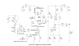
This is what is happening:
Green is coupling at the output with 10K Rin next
other are C between tube anode and high Rin of JFET buffer.
Schematic is in PDF

Maybe the direct coupling is not the best solution baring in mind that we have to C couple @ output? After the Coupling C at the very output is usually 10K as standard value for solid state input resistor. And it deserves by calculation min 10uF C. BUT that will reflect as loss of the "bottom of the harmonic content?
For the tube next stage the input resistor or pot is usually much larger value so this 10uF coupling C will be better suited...
.
For my opp. It is better to decouple after tube stage with say 10uF and with 1meg of input res for JFET high impednce input Buffer? The JFET buffer can be set for 0mV off-set output without need of Coupling C, so we stay with just one C in the chain, moderate value and dimmensions against the quality?
.
This is what is happening:
Green is coupling at the output with 10K Rin next
other are C between tube anode and high Rin of JFET buffer.
Schematic is in PDF
Attachments
Also I tried 4 sections of ECC88 (2 tubes) as tube part. Russian equivalent is also good. This is about 50mA/V of transconductance because in parallel of 12.5mA/V typical ECC88 per section.
Result is not bad at all?
I just take a look at the prices on e-bay for EC8020 (S=60mA/V) high transconductance tubes - I was pretty shocked😵. Please check...
So the 50mA/V for 4 x ECC88 sections are pretty afordable...
Maybe the 1.5V for the 2SK2394 JFET is just a bit from the knee? Should be better that not so close to the knee curves...
.
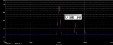
Very low THD. Consumption is about 53mA.
.
Result is not bad at all?
I just take a look at the prices on e-bay for EC8020 (S=60mA/V) high transconductance tubes - I was pretty shocked😵. Please check...
So the 50mA/V for 4 x ECC88 sections are pretty afordable...
Maybe the 1.5V for the 2SK2394 JFET is just a bit from the knee? Should be better that not so close to the knee curves...
.
Very low THD. Consumption is about 53mA.
.
Attachments
Finaly I had to "try" E55L (not so cheep but super affordable compared to EC8020) 🙂
also high transconductance tube, in triode mode S=50 mA/V
The -Ug can be 2.5V, 3V or higher, depending on Vb. That is above JFET knee point...
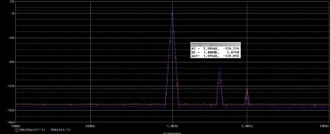
Result of spice sims are not so bad at all 🙂 as for the 88 too.
.
also high transconductance tube, in triode mode S=50 mA/V
The -Ug can be 2.5V, 3V or higher, depending on Vb. That is above JFET knee point...
Result of spice sims are not so bad at all 🙂 as for the 88 too.
.
Attachments
Many thanks Zoran guess I've open up another can of worms for myself to experiment. LolHi Sumotan, since many factors are in charge for value of the "signal integrity" resistor, as Fo, type of output of digital ICs, input capacitance of next in chain digital IC, and other things.
Best way is to put hands on scope and measure each connection point from beginning to the end.
Measure and trim for (i am using 220ohm trimpot to find the value replace with close standard value R ) absence of ringing at the edges of squares. You can round it a bit, bearing in mind HI and LO values for the specific IC.
One member did that as explained and report significant improvement in sound. I can say so, done it many times...
Hi Sumotan, since many factors are in charge for value of the "signal integrity" resistor, as Fo, type of output of digital ICs, input capacitance of next in chain digital IC, and other things.
Best way is to put hands on scope and measure each connection point from beginning to the end.
It's a lot more complex.
First let's separate critical signals (clocks that drive actual conversion) and uncritical signals (meaning als long as we get a correct 1/0 read in the permitted time we are good).
Clocks should use the fastest edge possible (though with something like tda1541 this rule has a clear upper slew rate limit), with back terminated transmission lines.and a correct clock tree.
Stubs must be avoided, but (for example) equal length double impedance splits in clock lines is permissible.
Which clock is actually the one that is critical to the conversion depends. On old style multi bit items is usually the word clock, on delta sigma it tends to be MCK.
It is possible to distribute a sinewave clockmall around a circuit board (ideally differential) and only square it up directly at the logic, but that's a lot of extra effort and making different clock squareres to be absolutely 100% in sync can be challenging.
ALL OTHER LINES can ignore impedance matched transmission lines and use significant series resistances. They should usually be matched in terms of resistor values, trace length and width but are not so critical on timing. Resistors should be as large as permissible to still allow correct function.
The slower the edge of the signal, the less EMI can be created. Less steep slopes will have less sharp switching on the IC's which is a mixed blessing. Tuning in circuit, with both GHz spectrum analyzer, audio analyser and even listening is recommended.
From experience usually the slowest slope that still works is best for ANYTHING except conversion clocks.
Thor
Maybe the direct coupling is not the best solution baring in mind that we have to C couple @ output? After the Coupling C at the very output is usually 10K as standard value for solid state input resistor. And it deserves by calculation min 10uF C. BUT that will reflect as loss of the "bottom of the harmonic content?
Well, on the DAC output DC coupling is pretty much mandatory. For 10K load I usually consider 2.2uF adequate, this gives 7Hz -3dB Point.
For my opp. It is better to decouple after tube stage with say 10uF and with 1meg of input res for JFET high impednce input Buffer? The JFET buffer can be set for 0mV off-set output without need of Coupling C, so we stay with just one C in the chain, moderate value and dimmensions against the quality?
I like DC coupled servo buffers mainly because a high quality 100nF capacitor is very easy to find and with a 1M bias resistor we get 1.6Hz -3dB.
Also I tried 4 sections of ECC88 (2 tubes) as tube part. Russian equivalent is also good. This is about 50mA/V of transconductance because in parallel of 12.5mA/V typical ECC88 per section.
Result is not bad at all?
Does increasing the transconductance from a single section, in the cascode part really have any material impact? And if so, why not use a Mosfet which will much higher transconductance?
Maybe the 1.5V for the 2SK2394 JFET is just a bit from the knee? Should be better that not so close to the knee curves...
Or maybe should be much lower? Maybe 0.5V for the J-Fet so it stays in triode region?
Finaly I had to "try" E55L (not so cheep but super affordable compared to EC8020) 🙂
also high transconductance tube, in triode mode S=50 mA/V
The -Ug can be 2.5V, 3V or higher, depending on Vb. That is above JFET knee point...
Result of spice sims are not so bad at all 🙂 as for the 88 too.
Try IRF710 and 48V "+B+.
Thor
@ThorstenL in your opinion, would paralleling two tda1541a be better done by dual mono approach (L+R in parallel per chip, and using counter shift register + digital multiplexer), or L+L and R+R in parallel from each chip? And in your opinion is it worth the trouble in comparison to using just one tda1541a? Thx.
Well, on the DAC output DC coupling is pretty much mandatory. For 10K load I usually consider 2.2uF adequate, this gives 7Hz -3dB Point.
Yes, by the calculations but take a look at the simulations somehow, FFT not reaching the lowest level? With increased C say a 100X that looking better.I like DC coupled servo buffers mainly because a high quality 100nF capacitor is very easy to find and with a 1M bias resistor we get 1.6Hz -3dB.
So in that terms is much more convenient to increase the C in 100nF/1meg coupling to 10uF/1meg
than in the 10uF/10K RC net at the output to 1000uF/10K...
With say JFET buffer set to 0mV offset it is possible to have direct conn to the output
So that 10uF is smaller and can be from better quality to try. As in the simulation FFT. 0.1uF VS 10uF.
It may would be interesting to listen to the chage?
As on the picture above few posts...
Does increasing the transconductance from a single section, in the cascode part really have any material impact? And if so, why not use a Mosfet which will much higher transconductance?
The high transconductance of the tube is not a must. But according to the simulations some higher S tubes behave better because they giving more "room" in Vds voltage to the JFET? Somehow higher Vds voltages below the jfet knee outputs better results.Or maybe should be much lower? Maybe 0.5V for the J-Fet so it stays in triode region?
The choice of this JFET is factor. Best by the spice models choices (not tested in real) are 2SK2394CP6 and BF861C. I will post results. With 2 2SK2394CP6 in parallel input resistance is about 16 ohms and flat to the MHZ region
For the tubes 5687 is very good, 6N6P also, 417A is OK, but ECC88 perform slightly better.
Output resistance is the same as RIV (anode load) resistance.
@ThorstenL in your opinion, would paralleling two tda1541a be better done by dual mono approach (L+R in parallel per chip, and using counter shift register + digital multiplexer), or L+L and R+R in parallel from each chip? And in your opinion is it worth the trouble in comparison to using just one tda1541a? Thx.
Unless you intend to add bit's below the LSB, paralleling or balanced operation has limited use.
A single TDA1541 correctly employed is at the limitations of the CD Format.
Thor
Yes, by the calculations but take a look at the simulations somehow, FFT not reaching the lowest level?
Simulation error? An AP2 does not show this.
The high transconductance of the tube is not a must. But according to the simulations some higher S tubes behave better because they giving more "room" in Vds voltage to the JFET? Somehow higher Vds voltages below the jfet knee outputs better results.
You can always add some voltage (negative or positive) to get the Vgs "just so"
The choice of this JFET is factor. Best by the spice models choices (not tested in real) are 2SK2394CP6 and BF861C. I will post results. With 2 2SK2394CP6 in parallel input resistance is about 16 ohms and flat to the MHZ region
You could always parallel multiple J-Fets.
For the tubes 5687 is very good, 6N6P also, 417A is OK, but ECC88 perform slightly better.
Output resistance is the same as RIV (anode load) resistance.
Of course, a cascode has very high output impedance.
I think using a folded cascode with a P-Mos would be a better choice, it allows an I/U conversion resistor to ground, if needed with DC offset to bias a DC coupled output buffer via a servo.
Thor
It is a bit complicated to make I2S line LL / RR datas. I did it once with some HEF logic. And it was not so bad, (Other DAC chip).@ThorstenL in your opinion, would paralleling two tda1541a be better done by dual mono approach (L+R in parallel per chip, and using counter shift register + digital multiplexer), or L+L and R+R in parallel from each chip? And in your opinion is it worth the trouble in comparison to using just one tda1541a? Thx.
But it was limited speed and deserves 8-12V supply for good operation. Because of "glue logic" used.
...
My tip is that the better way is to use Time Simultaneous format and feed 2 DAC channels inside the TDA1541A with a same data. That will be internal paralleled. DEM oscilator circuit is already the same for booth channels inside the chip.
.
I tried it, and somehow, for me, it was significantly better than I2S classic? (CPLD packed frmat for TDA1540 14bit and optionally 16bit for TDA1541A. Tried both sets.)
I also tried balanced mode with inverted data on other channel of TDA1541A and again, for me, it was not an impovement. It was more noise at measurements, and the sound become somehow "thin" with grainy highs... Balanced digital It is not as analog cancelation...
Yes that is the option. THe best way is to try, built, measure and listen. Expecially if that simple issue happens?Simulation error? An AP2 does not show this.
For some tubes that working with higher Io that has to be applied.You could always parallel multiple J-Fets.
For these Current sources in negative branch even more because of limitations of JFET Power.
Yes but in the multiplied DAC configurations Riv is proportionally smaller, leading to proportional significantly smaller output resistance. For the example of PCM1794A dac it is about 255 ohms because of the higher Io value.Of course, a cascode has very high output impedance.
I think using a folded cascode with a P-Mos would be a better choice, it allows an I/U conversion resistor to ground, if needed with DC offset to bias a DC coupled output buffer via a servo.
...
I run for the 2V p-p output voltage. Somehow 2Vrms (more than 5Vp-p) I found too much for the source to the for instance tube preamplifier?
So for TDA1540 and TDA1541A 4mAp-p @ 500ohms giving 2Vp-p output.
...
Again this Output voltage is in 180deg (opposite phase) and has to be corrected - in phase.
So basically no real benefit, at least not worth the effort and additional cost 🙂 One more question, you'd still prefer to go the route you did (on cd-77, schematic, i2s) or now you may think simultaneous might be better? I was thinking of making it as is by your schematic, not reinventing the wheel.Unless you intend to add bit's below the LSB, paralleling or balanced operation has limited use.
A single TDA1541 correctly employed is at the limitations of the CD Format.
Thor
@Zoran yes, lower output impedanse, no issue with modern devices, but in general, how did you like it, was it worth the additional investment?
"So basically no real benefit, at least not worth the effort and additional cost 🙂"
I can of course not claim to have all possible options etc.
But I tried a fair bit.
DIYHFS had both single and dual TDA1541 and single versions of what was the same design (other than double dac).
I preferred the single IC versions of otherwise identically modified and build up Machine's.
That doesn't invalidate other tests, but at the very best you messing around in the margins, if all else is equal.
Better focus on what helps most.
Thor
I spot something that might be of help. The lower JFET in the tube cathode is incrementing almost the exact about 13.5mA of current. So the multiplying of 2SK2394CP6 will multiply this 13.5mA of current.
Otherwise the 0mv @ Iinput from the DAC cant be set properly.
So the outcome is to adopt the settings and working point of the tube to n x 13.5mA point with minimum 1.5V -Ug point, (preferably 2 or 2.5 for -Ug). Va does not matter much and will be result of Ia and -Ug values...
Common JFET CCS in negative branch does not have bigger influences.
🙂
I will post the schs for different tubes.
.
This simple circuit behaves very very good with low values of Riv @ anode as 50ohms Harmonic content is almost the same as with 500ohm Riv. (Which is not the case with most diskrete IV topologies that a simulated with PSpice.)
- Home
- Source & Line
- Digital Line Level
- Building the ultimate NOS DAC using TDA1541A