•Still something confuse me. I found that EC change to use 50Hz about #6069.
Before that he try the higher freq DEM which I can get the point then.
The DEM accuracy seems to be better with high freq oscillator. But the low freq. modify do get better, why??
That he mention about facing some “DEM problem". But I wonder to know why it won’t cause some effect as it drop into the audible region.
I know this might discussed before but I’m sorry that I just can’t find it.
the other question is it seems to use two resistor at pin16 and pin17 connect to pin15
why change two a single registor?
It is a matter of high frequency noise from a high frequency DEM oscillator.
Why he changed to one resistor, I do not know, but apparently it does not make much difference, as there have been reports from members , that did the 50 Hz mod, but left two resistors in, and they report the same sonic improvement..
It sounds reasonable that reduce the high freq. noise.Maybe It's the dominate issue.
EC metioned several times about the glitch issue.
I'm not sure if I'm right about the higher the DEM freq the higher accuricy compensation it can give due to it's fomula in paper.But it might be some trade of I think comparing to the practical solution.
EC metioned several times about the glitch issue.
I'm not sure if I'm right about the higher the DEM freq the higher accuricy compensation it can give due to it's fomula in paper.But it might be some trade of I think comparing to the practical solution.
@ poki921.Hi sumotan,
This is caused by the I2S interface and the 200 KHz DEM clock, that's why I suggested to run the TDA1541A in simultaneous mode with 25% data density and use 50Hz DEM clock.
This reduces on-chip ground-bounce to almost zero when the outputs are latched, so it results in lowest obtainable jitter with this chip.
Here is what John said about exactly your question.
Hi SSerg,
DEM is required for averaging between 4 bit currents that have minor tolerances (matching of elements on the chip). It's all explained in the document that Alexandre posted. The goal is obtaining good matching bit currents from a circuit that has known tolerances.
In order to average between 4 slightly different bit currents, each corrected bit output current should represent the AVERAGE of all 4 input bit currents that have slight tolerances.
Suppose we have following INPUT bit currents:
Input bit current #1, 0.98mA
Input bit current #2, 0.92mA
Input bit current #3, 1.00mA
Input bit current #4, 0.90mA
And we use a switch matrix to connect each INPUT bit current to each output for 25% of a full DEM cycle:
25% of 0.98 + 25% of 0.92 + 25% of 1.00 + 25% of 0.90 = 0.95mA (output bit current #1)
25% of 0.92 + 25% of 1.00 + 25% of 0.90 + 25% of 0.98 = 0.95mA (output bit current #2)
25% of 1.00 + 25% of 0.92 + 25% of 1.00 + 25% of 0.90 = 0.95mA (output bit current #3)
25% of 0.90 + 25% of 0.98 + 25% of 0.92 + 25% of 1.00 = 0.95mA (output bit current #3)
Now we get 4 bit currents that have the same AVERAGE value, but with a ripple current that depends on the element matching:
Poor matching -> High ripple current.
Perfect matching -> No ripple current.
Since nothing is perfect there will be some ripple current and it is minimised by the active divider decoupling (lowpass filter) cap. The value of the filter cap is inverse proportional with the DEM frequency:
Low DEM frequency -> Big (high value) filter cap.
High DEM frequency -> Small (low value) filter cap.
All I did is reduce the DEM frequency, this will obviously lower the ripple current frequency too, so I simply used bigger (larger value) caps to take care of the lower ripple frequency, that's all.
There is no reason whatsoever why this averaging circuit would suddenly no longer work only because the switching frequency is changed.
If I would switch with 1Hz, it would now take 4 seconds to complete one DEM cycle and we would need Big electrolytic capacitors to filter out the 1 Hz ripple current.
If we would switch 1 million times a second, it would take 4us to complete one DEM cycle and we would only need a small capacitor to filter out the ripple current.
However, when increasing DEM clock rate we also increase the number of ground-bounces / second.
With 50Hz DEM I only have 50 ground-bounces / second. With 44.1 KHz sample rate this translates to one ground-bounce every 882 samples (no problem whatsoever).
With 1 MHz DEM I have 1 million ground-bounces a second. With 44.1 KHz sample rate this translates to 22.6 ground bounces WITHIN one sample.
The DEM switch matrix isn't perfect, the switches have finite switching time and each switch has tolerances in propagation time. At higher switch frequencies parasitics also start to play a major role.
The lower the DEM frequency, the lower the impact of switch timing tolerances on the generated average bit current.
With 50Hz DEM frequency, timing tolerances in DEM switches have virtually zero impact on accuracy. Bit accuracy is as high as it gets.
With 1 MHz DEM frequency, timing tolerances in the DEM switches and parasitics play a big role in bit accuracy. Bit accuracy will be poor, that's why Philips advised to use a DEM frequency that's not higher than roughly 200 KHz.
Knowing Philips they would have used 2MHz DEM clock and 10nF decoupling caps if this didn't cause any degrading as this saves cost (10nF caps are cheaper then 100nF caps).
Similar Philips would not have used lower DEM frequency because this requires bigger (more expensive) decoupling caps.
Finally, because there is on-chip crosstalk, DEM frequencies WITHIN the audio spectrum would become audible as very weak idle tones (I tested this). With 50Hz DEM I am at the low end of the audio spectrum and with this low DEM clock rate crosstalk is negligible as we only have one ground-bounce after every 882 samples.
Ground-bounce also leads to trigger uncertainty, so it is desirable to have fewest (preferably zero) ground-bounces the moment the TDA1541A outputs are latched. This gives lowest on-chip jitter.
--->>>> I included oscillograms of my prototype running on 50Hz DEM frequency in a previous post that prove that low level performance is superb, this would simply be impossible when DEM was not working perfectly. I left the DAC playing for a few days and re-tested low level performance, still perfect. Now you have some explaining to do 🙂
As explained this is not a very good idea. Many of us (me included) had moments where a distorted signal seemed to sound better to the ears.
And here yet another 😀
Hi
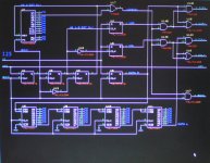
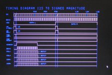
I have a couple of questions to the suggested I2S to signed magnitude proposed by John in post 6126:
The way the DOL- and DOR- is made with an AND gate and an OR gate , isen't it the same as just inverting the DOL+ and DOL+ ? I guess the reason for doing it the way John does is to avoid propagation delay between - data and + data?
But dosen't it then produce the infamous LSB error?
Another question is :
If I want to make a balanced DAC with signed magnitude TDA1541, I would have to have 4 TDA1541 and for the 2 TDA1541 producing the inverted analog signal, I just have to connect the DOR+ and DOL+ to Data L input and DOR- and DOL- to Data R input... Right?
Have anyone tried this at home?
Attachments
Hi
I have a couple of questions to the suggested I2S to signed magnitude proposed by John in post 6126:
The way the DOL- and DOR- is made with an AND gate and an OR gate , isen't it the same as just inverting the DOL+ and DOL+ ? I guess the reason for doing it the way John does is to avoid propagation delay between - data and + data?
But dosen't it then produce the infamous LSB error?
Another question is :
If I want to make a balanced DAC with signed magnitude TDA1541, I would have to have 4 TDA1541 and for the 2 TDA1541 producing the inverted analog signal, I just have to connect the DOR+ and DOL+ to Data L input and DOR- and DOL- to Data R input... Right?
Have anyone tried this at home?
Does the TDA1541 operate with Signed Magnitude Binary? As far as I know it needs either Twos complement, or Offset Binary in mux or simultaneous mode.
SMB needs an extra bit for the sign so you need a way of generating this?
Does the TDA1541 operate with Signed Magnitude Binary? As far as I know it needs either Twos complement, or Offset Binary in mux or simultaneous mode.
SMB needs an extra bit for the sign so you need a way of generating this?
look at the post I pointed to. John has made a circuit so that TWO tda 1541 can work AS signed magnitude.
Last edited:
I have been studying this Signed Magnitude converter a couple of times, and finally I got the point.
To explain it in a more common language:
John uses one TDA1541 for each channel. Lets call the two DAC´s inside for the positive DAC (DAC+) and the negative DAC (DAC-). The output from these two DAC's are connected together and form one of the two stereo cannels.
Lets just look at the right channel.
The converter looks for the MSB to see if it is 1 or 0 and this controls the data stream to the two DAC'S(DAC+ and DAC-). If MSB is 1, DAC+ gets data, while DAC- does not get any data. If MSB is 0 DAC- gets data and DAC+ does not get any data.
The data the two DAC's (DAC+ and DAC- ) receives is selected by the window generator in the converter . This selects 16 bits , but not the normal 16 bits from bit 1 to 16, but bit 2 to bit 17...
So MSB controlles witch DAC (DAC+ or DAC-) is active (this now becomes MSB in the combined DAC (DAC+ and DAC-)) and the data clocked in to these two DAC's (you know by now ;-)) is bit 2 to 17 . And voila a 17 bit DAC with no zero crossing problem.
The rest of the converter is doing the job of delaying the Left data so the Left DAC (consisting of two DAC's , DAC+ and DAC -) receives them simultaneous with the Right channel.
Most of you probably have grabbed this a long time ago, but it was a good exercise for me to write it down, and perhaps someone can benefit from it (I hope 😱)
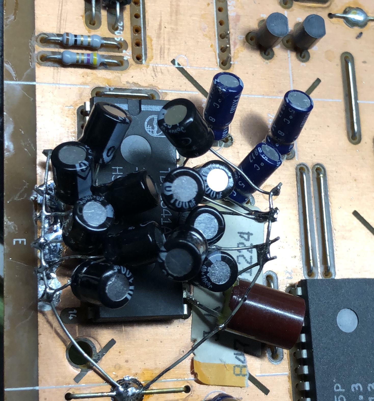
I know how ugly it looks
But here’s the contribution of it
It use the cheap caps obviously not the great grounding
But still good sounds without problems🙂
Last edited:
GRM31CR61E476ME44K Murata Electronics | Mouser 臺灣
Did any one used the MLCC CAP 1206 for replacement the DEM decoupling cap before?
Did any one used the MLCC CAP 1206 for replacement the DEM decoupling cap before?
koldby, thanks for the clear explanation. It is not clear (at least for me) how the analog outputs of DAC+ and DAC- are combined, knowing that both has -2 mA to 0 mA output.
I have been studying this Signed Magnitude converter a couple of times, and finally I got the point.
To explain it in a more common language:
John uses one TDA1541 for each channel. Lets call the two DAC´s inside for the positive DAC (DAC+) and the negative DAC (DAC-). The output from these two DAC's are connected together and form one of the two stereo cannels.
Lets just look at the right channel.
The converter looks for the MSB to see if it is 1 or 0 and this controls the data stream to the two DAC'S(DAC+ and DAC-). If MSB is 1, DAC+ gets data, while DAC- does not get any data. If MSB is 0 DAC- gets data and DAC+ does not get any data.
The data the two DAC's (DAC+ and DAC- ) receives is selected by the window generator in the converter . This selects 16 bits , but not the normal 16 bits from bit 1 to 16, but bit 2 to bit 17...
So MSB controlles witch DAC (DAC+ or DAC-) is active (this now becomes MSB in the combined DAC (DAC+ and DAC-)) and the data clocked in to these two DAC's (you know by now ;-)) is bit 2 to 17 . And voila a 17 bit DAC with no zero crossing problem.
The rest of the converter is doing the job of delaying the Left data so the Left DAC (consisting of two DAC's , DAC+ and DAC -) receives them simultaneous with the Right channel.
Most of you probably have grabbed this a long time ago, but it was a good exercise for me to write it down, and perhaps someone can benefit from it (I hope 😱)
Forgot to mention that the data to the DAC- is inverted. And -no- you can not just swap the DOL+ and DOL- to get an inverted signal out. It makes no change. You must either invert all the data lines (DOR+, DOR- , DOL+ , DOL-) or invert the sampled MSB out of U4 and U5 and the feed that to a duplicate of the AND and OR gate complex U14 , U15 and U16 in order to get the same propagation delay for the inverted DAC's.
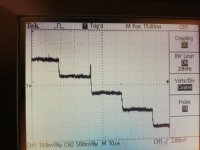
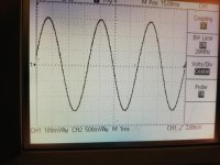
Attached: the second picture is a picture of a 5% full scale digital 300 Hz sinus from a TDA1541A running simultaneous mode with stopped clock.
The first is a closeup of that around the zero crossing. It is easy to see the big spike, when TDA1541A is changing all the bits at once. No spikes on any of the other transisions. Good reason to try Sign Magnitude 😀
Attachments
Did any one used the MLCC CAP 1206 for replacement the DEM decoupling cap before?
I'd be concerned about a couple of things with these. First they're nonlinear having a substantial capacitance change with voltage. Second, they're microphonic - but then again, so are electrolytics.
Hi koldby,
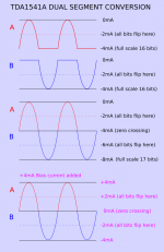
I attached a drawing that explains how both TDA1541A D/A converter segments are combined.
Segment A = TDA1541A #1 L channel (DOL+)
Segment B = TDA1541A #1 R channel (DOL-)
Same for the other stereo channel
Segment A = TDA1541A #2 L channel (DOR+)
Segment B = TDA1541A #2 R channel (DOR-)
All bits of each converter / segment flip @ -2mA, this is fixed inside the chip and cannot be changed externally. Using a single chip, all bits would flip at the critical zero crossing (-2mA).
Because the MSBs are now also included for low level signal generation we need extreme accuracy for these MSBs (this is one of the problems with multibit converters).
The audibility of bit errors is most noticeable at low signal levels (around the zero crossing area) where small bit errors will no longer be masked by much louder signals.
The segmented mode fixes this, all bits will no longer flip around the critical zero crossing but halfway between the zero crossing and signal maximum where the TDA1541A output current equals -2mA.
The MSBs are no longer needed for -dynamic- low level signal generation. The MSBs now only apply a static DC current. Bit errors in the MSBs only translate to very small DC-offset current in the zero crossing area (0 ... +1023 and 0 ... -1023).
Low level performance depends on the bit errors in the passive dividers (10 bits) only. When the bit errors in these 10 bit passive dividers are say 0.1 LSB then we get 0.1 LSB error in the range of -1023 ... +1023 while the total LSB error (MSBs included) could be say 1 LSB over the full scale as specified in the datasheet.
The circuit I posted will not produce a 1LSB error but only a fixed 0.5 LSB error around the zero crossing. The LSB of each segment (A or B) will now represent 0.5 LSB. Because of the coding scheme, one LSB of one segment (representing 0.5 LSB) is added, so we end up with 0.5 LSB error instead of 1 LSB error.
The error is a result of a double zero code around the zero crossing that results in a 1 LSB error if not corrected.
Single plain A TDA1541A will produce a similar 0.5 LSB error or even higher depending on chip grading, plus the bit switching noise plus the ripple current noise on the MSBs.
So even with comparable bit error, things will improve significantly because there is less switching noise and less ripple current around the signal zero crossing area.
But when we let the other (still unused) bit 16 of the other segment follow MSB of the I2S input stream, this error is fully compensated by adding another LSB (now total of 1 LSB is added). We now end up with a converter that offers improved low level performance and very low (switching) noise. This cannot be achieved using a single TDA1541A.
The way the DOL- and DOR- is made with an AND gate and an OR gate , isen't it the same as just inverting the DOL+ and DOL+ ? I guess the reason for doing it the way John does is to avoid propagation delay between - data and + data?
But dosen't it then produce the infamous LSB error?
I attached a drawing that explains how both TDA1541A D/A converter segments are combined.
Segment A = TDA1541A #1 L channel (DOL+)
Segment B = TDA1541A #1 R channel (DOL-)
Same for the other stereo channel
Segment A = TDA1541A #2 L channel (DOR+)
Segment B = TDA1541A #2 R channel (DOR-)
All bits of each converter / segment flip @ -2mA, this is fixed inside the chip and cannot be changed externally. Using a single chip, all bits would flip at the critical zero crossing (-2mA).
Because the MSBs are now also included for low level signal generation we need extreme accuracy for these MSBs (this is one of the problems with multibit converters).
The audibility of bit errors is most noticeable at low signal levels (around the zero crossing area) where small bit errors will no longer be masked by much louder signals.
The segmented mode fixes this, all bits will no longer flip around the critical zero crossing but halfway between the zero crossing and signal maximum where the TDA1541A output current equals -2mA.
The MSBs are no longer needed for -dynamic- low level signal generation. The MSBs now only apply a static DC current. Bit errors in the MSBs only translate to very small DC-offset current in the zero crossing area (0 ... +1023 and 0 ... -1023).
Low level performance depends on the bit errors in the passive dividers (10 bits) only. When the bit errors in these 10 bit passive dividers are say 0.1 LSB then we get 0.1 LSB error in the range of -1023 ... +1023 while the total LSB error (MSBs included) could be say 1 LSB over the full scale as specified in the datasheet.
The circuit I posted will not produce a 1LSB error but only a fixed 0.5 LSB error around the zero crossing. The LSB of each segment (A or B) will now represent 0.5 LSB. Because of the coding scheme, one LSB of one segment (representing 0.5 LSB) is added, so we end up with 0.5 LSB error instead of 1 LSB error.
The error is a result of a double zero code around the zero crossing that results in a 1 LSB error if not corrected.
Single plain A TDA1541A will produce a similar 0.5 LSB error or even higher depending on chip grading, plus the bit switching noise plus the ripple current noise on the MSBs.
So even with comparable bit error, things will improve significantly because there is less switching noise and less ripple current around the signal zero crossing area.
But when we let the other (still unused) bit 16 of the other segment follow MSB of the I2S input stream, this error is fully compensated by adding another LSB (now total of 1 LSB is added). We now end up with a converter that offers improved low level performance and very low (switching) noise. This cannot be achieved using a single TDA1541A.
Attachments
Forgot to mention that the data to the DAC- is inverted. And -no- you can not just swap the DOL+ and DOL- to get an inverted signal out. It makes no change. You must either invert all the data lines (DOR+, DOR- , DOL+ , DOL-) or invert the sampled MSB out of U4 and U5 and the feed that to a duplicate of the AND and OR gate complex U14 , U15 and U16 in order to get the same propagation delay for the inverted DAC's.
Attached: the second picture is a picture of a 5% full scale digital 300 Hz sinus from a TDA1541A running simultaneous mode with stopped clock.
The first is a closeup of that around the zero crossing. It is easy to see the big spike, when TDA1541A is changing all the bits at once. No spikes on any of the other transisions. Good reason to try Sign Magnitude 😀
Thanks for that explanation, I too now understand ECD's approach. I will be closely examining the outputs from my balanced dac next week although I do not know how IanCanada's dsp chip generates the bit perfect inverted data.
Hi John
Thanks for clarifying that. Could you comment on my thoughts on using 4 TDA1541 in a balanced Sign Magnitude DAC. Is it ok to just use inverters on all the 4 datalines (DOL+, DOL- DOR+ DOR-) or should I use the approach with inverting the sampled MSB and build a copy of the AND- OR complex U14 , U15 and U16 ?
Thanks for clarifying that. Could you comment on my thoughts on using 4 TDA1541 in a balanced Sign Magnitude DAC. Is it ok to just use inverters on all the 4 datalines (DOL+, DOL- DOR+ DOR-) or should I use the approach with inverting the sampled MSB and build a copy of the AND- OR complex U14 , U15 and U16 ?
The TDA1541 produces -4mA to 0 mA. So if you combine two you get -8mA to 0 mA. Midt point (no data to either DAC) will result in -4 mA.koldby, thanks for the clear explanation. It is not clear (at least for me) how the analog outputs of DAC+ and DAC- are combined, knowing that both has -2 mA to 0 mA output.
So only one of the DAC's change output if the data is anything else than zero's
DAC+ adds to the -4 mA when the MSB is 1 and DAC- subtract from the -4mA when MSB is 0. Providing a bias of +4 mA to the joint output of the two DAC's results in a output of +4mA to - 4mA. Look at Johns drawing.
- Home
- Source & Line
- Digital Line Level
- Building the ultimate NOS DAC using TDA1541A