Hi batteryman,
Philips TDA1541A datasheet page 4
quote:
When input OB/TWC input is connected to VDD1 the two channels of data (L/R) are input simultaneously via DATA L and DATA R, accompanied with BCK and a latch-enable input (LE). With this mode selected the data must be in offset binary. The converted samples appear at the output at the positive going transition of the latch enable signal.
The format of the data input signals is shown in Fig.5 and 6.
When you invert LE, the positive going transition (latching) will occur -after- all bits have been clocked in. This would meet datasheet specs and should work.
See attached modified oscillogram.
Yes it should work, but why haven't Ian's customers who have used his converter with a 1541 not had the same issue?
There's only one way to find out..
I don't think so. TDA1541A can operate at 14 bits just like TDA1540 and it does work just fine. You wouldn't hear any difference between 14 bits and 16 bits.
I can imagine there is another issue. Can you show us the DATA line (whether it's R or L, doesn't matter) along with BCLK on the same screen? If you can include 3rd graph of LE that would be lovely, but that's not necessary.
Here are two traces: Data + BCK and Data + LE
Attachments
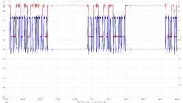
I can only assume that the red on the first picture is DATA and blue is BCK. You wouldn't hear a difference between 14/15 and 16 bits, so I knew that wasn't the case. Anyway, I thought so. You can see it's completely wrong. TDA1540 as well as TDA1541 clocks data in on the falling edge of the BCK. Not on the rising edge of BCK like other DACs.
DATA on your graph changes with the falling edge of BCK which means its justified for clocking in data on the rising edge like normal DACs do require it to be. However, that's not the case with TDA1540 and TDA1541.
Check this out:
http://www.lampizator.eu/lampizator/LINKS AND DOWNLOADS/DATAMINING/tda 1541A.pdf

You can see that DATA needs to change on the rising edge of the BCLK, so it should be stable for the falling edge which clocks it in.
DATA on your graph changes with the falling edge of BCK which means its justified for clocking in data on the rising edge like normal DACs do require it to be. However, that's not the case with TDA1540 and TDA1541.
Check this out:
http://www.lampizator.eu/lampizator/LINKS AND DOWNLOADS/DATAMINING/tda 1541A.pdf
You can see that DATA needs to change on the rising edge of the BCLK, so it should be stable for the falling edge which clocks it in.
I can only assume that the red on the first picture is DATA and blue is BCK. You wouldn't hear a difference between 14/15 and 16 bits, so I knew that wasn't the case. Anyway, I thought so. You can see it's completely wrong. TDA1540 as well as TDA1541 clocks data in on the falling edge of the BCK. Not on the rising edge of BCK like other DACs.
DATA on your graph changes with the falling edge of BCK which means its justified for clocking in data on the rising edge like normal DACs do require it to be. However, that's not the case with TDA1540 and TDA1541.
Check this out:
http://www.lampizator.eu/lampizator/LINKS AND DOWNLOADS/DATAMINING/tda 1541A.pdf
You can see that DATA needs to change on the rising edge of the BCLK, so it should be stable for the falling edge which clocks it in.
Yes I agree it is wrong but yet it sounds okay until there is a peak. (I do have the datasheet)
You'd never suspect a problem if the recording was done at a lower level or the track was of quiet music.
I have tried using half speed mode and also 18 & 20bit settings and none make any difference either to the distortion or to what I can see on the scope.
I'm afraid there will be many more audible artifacts due to bits swapping, but your brain simply told you that this is how it sounds "right" and different from I2S mode due to those errors.
Your issue happens because MSB (sign bit) is overlapped and you hear some crackles due to signal switching its sign from intended value. It happens to other bits, too, so you might hear certain parts louder than others depending on the luck how the bit swaps its place.
Your issue happens because MSB (sign bit) is overlapped and you hear some crackles due to signal switching its sign from intended value. It happens to other bits, too, so you might hear certain parts louder than others depending on the luck how the bit swaps its place.

Hmmm..It's an LSB error. The idea for a differential output is to cancel any even harmonics and for that the amplitude needs to be precisely matched in terms of the magnitude to work as expected and to cancel out at low leveled signals.
This won't be much of an issue obviously, but lets not treat it as just "DC error" because it's not.
I will probably use a trafo to balance the output from the DAC, so it is a little bit theoretical, but...
If I treat it like a DC error and adjust both dacs to 0 Vdc with no data in, I will , as far as I can tell, get perfect balance (lets not talk montomy issues here) until the data reaches fullscale minus 1bit...That will , for all normal music , never happen.
I would have to ensure the bias circuit is capable of putting out at least 2 mA, very low noise , very stable and adjustable to a precision of at least 17 bits. How to do that..?
A current out DAC of course 😀.
And preferrable a r2r or other multibit DAC, as Delta Zigma versions need to have a constant refreshment of its current out stage. Could be done with a Delta Zigma, but one has to isolate it very well to avoid issues with digital noise from the necessary clock.
So two parrallel PCM 1704 to make the bias for each TDA 1541A. That would be a nice treat...😀😀😀
Put a NOT gate on BCK from Ian's board to TDA1541A and see if it changes anything.
I'll give it a go, what about inverting LE?
I'll give it a go, what about inverting LE?
FWIW I have Ian's board and two Red Baron TDA1541A boards and they work fine together..
FWIW I have Ian's board and two Red Baron TDA1541A boards and they work fine together..
What is your I2S source?
Yes I can't believe Ian's board has a design flaw so I think it maybe be the I2S input its receiving?
It's from a Toshiba CD/MP3 single chip cd processor ( which does it all from transport to dac). It has an internal dac as well but this is not used, the I2S goes to a PCM1901a 24bit dac.
I think my next step is to get the I2S from the inputs to a SAA7220 in an old Marantz Cd player and see what happens.
I will , as far as I can tell, get perfect balance (lets not talk montomy issues here) until the data reaches fullscale minus 1bit...That will , for all normal music , never happen.
You will be off one LSB for every signal and not just the fullscale.
It happens because the inversion of a signal is actually NOT+1 and not just NOT. It means that after inverting all bits within the signal to get inversion you have to add +1 to it.
That is true for 2s complement:
Code:
01100100 = 100
NOT
10011011 = -101
+1
10011011 + 1 = 10011100 = -100
Two's Complement Calculator | Online Conversions
I'll give it a go, what about inverting LE?
Leave it as it is for now, we will worry about it later on. If I'm right inverting LE will cause the TDA1541A to clean up input register before latching due to negative transition of LE during clocking, so you won't get any useful data out of the DAC. On the other hand loosing one LSB bit is hardly an issue.
koldby said:If I treat it like a DC error
If I treat a cat like a dog, it doesn't stop being a cat.
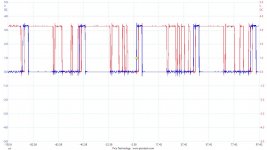
Here's a screen shot of the latch and bck, which look okay to me and of course you can see the clock stop feature of Ian's interface.
I will try half speed mode next and if that doesn't help, I'll move the interface into a Marantz Cd65 1541 based cd player.
I think that is not correct - LE should be one CLK delayed? It is going into conversion before LSB.
Here are two traces: Data + BCK and Data + LE
From this it look like the 1/2 of MSB lost? The SYS CLK is from rising edge and it has 16 cycles. That is good. The Word is finishing at the BCK end. But the 1st 1/2 of MSB missing...
So with LE with LSB and this, You loosing MSB and LSB, and probably something else is happening wrong.
BCK is have to be delayed by one self cycle or 4/2 MCK periods to line up with datas. That is depends of MCK timing. That is 2 x FlipFlop clocked with MCK input is BCK out is Q from the 2nd FF...
After that You can use 3 x flopflop 74 clocked with BCK for LE to move 1.5 BCK period and recover LSB. 1.5 or 3/2 of BCK You are alredy miss 1/2 BCK at LE, and with delay of 1 BCK for MSB recovery that will be 3/2 of BCK
cheers
Last edited:
Well I know that, but isen't that what I just did (adding 1 to the number) by setting the BIAS to what is equal to 1 LSB , for the inverted DAC ?You will be off one LSB for every signal and not just the fullscale.
It happens because the inversion of a signal is actually NOT+1 and not just NOT. It means that after inverting all bits within the signal to get inversion you have to add +1 to it.
That is true for 2s complement:
Code:01100100 = 100 NOT 10011011 = -101 +1 10011011 + 1 = 10011100 = -100
If I treat a cat like a dog, it doesn't stop being a cat.
Well maybe he starts believing he is a dog , if you do it long enough 😛
Last edited:
I have used Mini dsp xmos based usb streamer and DIYinhk xmos based USB receiver. Both worked perfectly. You say PCM1901A , I am not able to find anything about that. Are you sure it is a I2S signal you have there?What is your I2S source?
Yes I can't believe Ian's board has a design flaw so I think it maybe be the I2S input its receiving?
It's from a Toshiba CD/MP3 single chip cd processor ( which does it all from transport to dac). It has an internal dac as well but this is not used, the I2S goes to a PCM1901a 24bit dac.
I think my next step is to get the I2S from the inputs to a SAA7220 in an old Marantz Cd player and see what happens.
Last edited:
Well I know that, but isen't that what I just did (adding 1 to the number) by setting the BIAS to what is equal to 1 LSB , for the inverted DAC ?
Ahh yea, I didn't read that part. Well, in general that will work, but if you go into details that LSB offset should be in fact generated by the DAC itself, so the nonlinearity errors of that DAC match with the non-inverting DAC.
Lets be clear on that though - you won't be able to hear any difference on that LSB, but from a technical point of view certain issues might visible on very low-leveled signals.
- Home
- Source & Line
- Digital Line Level
- Building the ultimate NOS DAC using TDA1541A