Bit0-Bit15, I count 16 bits resolution. The challenge is an output stage wehre the lower bits aren't swamped by noise.
Most music hirez or otherwise only has a few bits resolution, a dynamic range on a commercial recording of 40db ~ 7 bits would be exceptional. Probalably the reason most of us reading this thread understand the TDA1541A understand the old sayin "its the first watt that matters most."
Thanks Regal,
This would help to explain the perceived SQ. With less than ideal caps wrt leakage (8.2uf /3uA), it was hard to reconcile that the sound was so much better including substantially increased micro detail & quiet background over the 220nf film. Perhaps I am losing the least significant 5 bits, but they carry no practical information? It would be interesting to do an A/B test, but that is not easy given the need for mm signal path. Perhaps 2 caps soldered to the MSB and A/B on the ground return wire.
I've used capacitors with more leakage than 3µA on the MSB pins and not measured any degradation (1Khz -60dbFS) atleast nothing coresponding to losing that many bits of resolution.
EC's Jitter Atten
Hi EC,
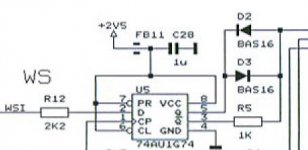
Could you please explain about this circuit? I'm thinking of for days but don't understand how it work and its effect. I used 74HC175 for reclocking in my TDA1541A DAC so far and would try apply your circuit on. But I don't understand it well.
Thx and Rdgs,
Art.
Hi EC,
Could you please explain about this circuit? I'm thinking of for days but don't understand how it work and its effect. I used 74HC175 for reclocking in my TDA1541A DAC so far and would try apply your circuit on. But I don't understand it well.
Thx and Rdgs,
Art.
Attachments
Art,
Have a read of this then write out a truth table. It helped me understand.
http://docs-asia.electrocomponents.com/webdocs/0cb4/0900766b80cb4d8f.pdf
Have a read of this then write out a truth table. It helped me understand.
http://docs-asia.electrocomponents.com/webdocs/0cb4/0900766b80cb4d8f.pdf
Thanks, ryanj. I understand how the flipflop work but don't understand after the flipflop. If I miss something, please point me out.
Art,
As far as i understand it, D2, D3, and R5 are the parts attenuating the signal.
Q and Q not, would cancel each other out if R5 was not there, but because of R5 there is slightly more voltage from pin 5 to DAC as a result.
As far as i understand it, D2, D3, and R5 are the parts attenuating the signal.
Q and Q not, would cancel each other out if R5 was not there, but because of R5 there is slightly more voltage from pin 5 to DAC as a result.
Thanks, ryanj. I understand how the flipflop work but don't understand after the flipflop. If I miss something, please point me out.
The diodes clamp the voltages limiting the voltage swing as seen from the TDA, the resistor limits the slew rate on negative going edges.
Dear -EC-,
I am thinking about converting my DI-16, now DI-4, into a passive balanced output DAC. Now I am confused: how do I connect the new low noise voltage reference for the negative outs?
I hope you can enlight me.
Thanks in advance.
M.
I am thinking about converting my DI-16, now DI-4, into a passive balanced output DAC. Now I am confused: how do I connect the new low noise voltage reference for the negative outs?
I hope you can enlight me.
Thanks in advance.
M.
Hi QSerra Tico Tico, not this exactly. I use a gas kitchen fire. I take the chip or the device of my interest with an universal plier, and I put the chip very very near the fire, touching it, for some seconds, even some minutes, and with the extractor fan on, and I wait until the chip plastic becomes a little "white". Then I let it on a plate and wait some minutes until it cools, and then, with my fingers, under running water, very carefully I remove the plastic until I can see the chip. I clean the rests of plastic and I finish extracting the rest of plastic and clean it with water. Maybe the first pieces you try don't work, but with a little practice you finally can do it without problem. It's like solder. Last day I've solded the 4 flip flop smd for the TDA1541A signal treatment of John's design. Because I have more than 21 years in soldering I can do it without problems and quickly. See enclosed photo of my Philps CD player of the 85'. Yes, I now it's a dirty job, but it's sound is incredible now. You can see from top to down: audio out, signal tratment, and my clock, not the last version, but a good one (-171dbc/hz). And respect to the treatmen signal pcb, you can see near the 1206 resistors the chips. Yes I now the resistors are big, but I hadn't at hand other components.
PD: John, thank you very much for your knowledge and for sharing it with us.
Now the CD player sounds with a silence level that remains me a turntable. The detail level, tonal precision, naturality and soundstage is now as real as real music.
Galeb,
Impressive I must say!
As I will be going on this route over the next couple of weeks, I would be very interested in your clock design/layout...
-which did you use?
-how does it perform compared to solutions like Tent?
-what type of power regulation did you feed to the clock?
Thanks!
Clock things
Hi Studiostevus,
My clock design is an optimized Colpits oscillator. Because I have access to a simmetricon tester, I can see how does my clock perform. To design it, I use a special software, and I've adjusted the simulation to have an error of +-1dbc/hz respect to the real design.( The pcb design layout is done with this same software, wich one is used to design pcb's for cellular phones).
The supply has to be clean. I use 3 inductors of 1mh each, and 4 capacitors, the 2 firsts of 1000uf and the last ones of 10nf, forming an RC filter. All this section after a regulator of 9vdc, and 2 capacitors of 4.700uf, one before and the other after the regulator. I use the BFR92 for the oscillator. Special care must be taken when choosing the 2 capacitors for the crystal feedback, because of these ones, it depends a lot the noise quality of the design.
For now, I've reached -183,5 dbc/hz in my last design, and 0,2ppm with a fast discrete temperature control.
Don't know how does the Tent clock performs, but I've experienced that very low phase noise is vastly more important than very low ppm.
Sorry, but I can't post schematics, this is a research work for an audio company and it has copyright.
Hope this helps a little. 😉
Could someone please post the current versions of the schematics? I really like this design. I'll try to build it if I can source the parts. I started reading trough this thread and I could use all the diagrams in one place to follow it easier.
For now, I've reached -183,5 dbc/hz in my last design, and 0,2ppm with a fast discrete temperature control.
Thats very impressive!
LClock XO3 = -153 dbc/Hz
Tent clock = http://www.diyaudio.com/forums/digi...44mhz-low-jitter-clock-kit-8.html#post1804962
Maybe this article will be useful...🙂
http://repository.tudelft.nl/assets/uuid:283c827b-7257-461a-9fce-b0c2e3b6f99f/TR-diss-1781.pdf
http://repository.tudelft.nl/assets/uuid:283c827b-7257-461a-9fce-b0c2e3b6f99f/TR-diss-1781.pdf
Hi Art,
The circuit attenuates I2S signals to low level signals that can still reliably drive the I2S inputs of the TDA154x. TDA154x has current mode I2S inputs that are compatible with 5V TTL signals.
By minimizing signal amplitude, less RF energy is dumped into the chip internal circuits (reduced ground-bounce). This in turn helps to reduce related on-chip jitter levels.
In the MK7, BCK attenuator is driven by a divide-by-4 circuit and DATA / WS are driven by synchronous reclockers.
The I2S attenuator circuit is driven by an ultra high speed flip-flop running at approx. 2.4V power supply. Fast logic runs on lower power supply voltages in order to reduce losses / interference.
The voltage drop across the diodes equals 0.6V typical.
Output is logical zero, Q = 0, /Q = 1:
/Q tries to put 2.4V on the output through R5 (1K), but Q pulls this voltage down to 0.6V (D2 conducts). The output voltage for logical zero now becomes 0.6V.
Output is logical one, Q = 1, /Q = 0:
/Q tries to pull the output to 0V, but Q pulls it high (D3 conducts). However, the voltage drop across D3 will limit output voltage to 2.4 - 0.6 = 1.8V.
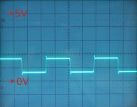
So the attenuator output will swing between 0.6V (logical zero) and 1.8V (logical one). The output signal amplitude equals 1.8 - 0.6 = 1.2Vpp. I attached a picture showing the BCK output signal.
I use these I2S attenuators on all I2S signals, BCK, WS and DATA.
Could you please explain about this circuit? I'm thinking of for days but don't understand how it work and its effect.
The circuit attenuates I2S signals to low level signals that can still reliably drive the I2S inputs of the TDA154x. TDA154x has current mode I2S inputs that are compatible with 5V TTL signals.
By minimizing signal amplitude, less RF energy is dumped into the chip internal circuits (reduced ground-bounce). This in turn helps to reduce related on-chip jitter levels.
In the MK7, BCK attenuator is driven by a divide-by-4 circuit and DATA / WS are driven by synchronous reclockers.
The I2S attenuator circuit is driven by an ultra high speed flip-flop running at approx. 2.4V power supply. Fast logic runs on lower power supply voltages in order to reduce losses / interference.
The voltage drop across the diodes equals 0.6V typical.
Output is logical zero, Q = 0, /Q = 1:
/Q tries to put 2.4V on the output through R5 (1K), but Q pulls this voltage down to 0.6V (D2 conducts). The output voltage for logical zero now becomes 0.6V.
Output is logical one, Q = 1, /Q = 0:
/Q tries to pull the output to 0V, but Q pulls it high (D3 conducts). However, the voltage drop across D3 will limit output voltage to 2.4 - 0.6 = 1.8V.
So the attenuator output will swing between 0.6V (logical zero) and 1.8V (logical one). The output signal amplitude equals 1.8 - 0.6 = 1.2Vpp. I attached a picture showing the BCK output signal.
I use these I2S attenuators on all I2S signals, BCK, WS and DATA.
Attachments
Hi Tazz,
If these caps indeed have 3uA leakage current, it is almost 50 times higher compared to the 0.061uA LSB current.
Problem is that the leakage current on the 6 MSBs (active dividers) won't be exactly the same and that the 10 LSBs (passive dividers) don't have this leakage current at all.
The result could be significant loss of (dynamic) resolution (up to 5 bits).
I've used capacitors with more leakage than 3µA on the MSB pins and not measured any degradation (1Khz -60dbFS) atleast nothing coresponding to losing that many bits of resolution.
If these caps indeed have 3uA leakage current, it is almost 50 times higher compared to the 0.061uA LSB current.
Problem is that the leakage current on the 6 MSBs (active dividers) won't be exactly the same and that the 10 LSBs (passive dividers) don't have this leakage current at all.
The result could be significant loss of (dynamic) resolution (up to 5 bits).
Hi maxlorenz,
The negative outputs are just in anti-phase, DC voltage levels remain the same as with the in-phase outputs.
So you can use one reference for all 4 passive I/V resistors. So all 4 passive I/V resistors connect to this single voltage reference. L, /L, R and /R signals are tapped from these 4 resistors.
If you also want to add full-DC-coupling, an extra variable DC reference voltage is required that will then serve as "GND reference", similar as with the MK7 DAC. This voltage needs to be fine-tuned so it exactly matches DC level on the 4 outputs.
I am thinking about converting my DI-16, now DI-4, into a passive balanced output DAC. Now I am confused: how do I connect the new low noise voltage reference for the negative outs?
The negative outputs are just in anti-phase, DC voltage levels remain the same as with the in-phase outputs.
So you can use one reference for all 4 passive I/V resistors. So all 4 passive I/V resistors connect to this single voltage reference. L, /L, R and /R signals are tapped from these 4 resistors.
If you also want to add full-DC-coupling, an extra variable DC reference voltage is required that will then serve as "GND reference", similar as with the MK7 DAC. This voltage needs to be fine-tuned so it exactly matches DC level on the 4 outputs.
Similar to the bias voltage used in Pedja's output stage (using 2sk170) I presume.If you also want to add full-DC-coupling, an extra variable DC reference voltage is required that will then serve as "GND reference", similar as with the MK7 DAC. This voltage needs to be fine-tuned so it exactly matches DC level on the 4 outputs.
As a intellectual exercise, I have also been wondering whether it wouldn't be possible to replace the 2sk216 on the output stage with a tube... haven't really thought about it any further though
Sorry I should point what it is about...
this is article:
HIGH-SPEED AND HIGH-RESOLUTION ANALOG-TO-DIGITAL AND DIGITAL-TO-ANALOG CONVERTERS
by
Rudy J. van de Plassche
.
something that could be connected with this thread?
84Mb file
cheers
this is article:
HIGH-SPEED AND HIGH-RESOLUTION ANALOG-TO-DIGITAL AND DIGITAL-TO-ANALOG CONVERTERS
by
Rudy J. van de Plassche
.
something that could be connected with this thread?
84Mb file
cheers
I scanned the article some days ago (it was posted elsewhere as well), and i find it great! It really contributes to my understanding of the workings of the chip (tda1540/1) and its implementations
The negative outputs are just in anti-phase, DC voltage levels remain the same as with the in-phase outputs.
So you can use one reference for all 4 passive I/V resistors. So all 4 passive I/V resistors connect to this single voltage reference. L, /L, R and /R signals are tapped from these 4 resistors.
If you also want to add full-DC-coupling, an extra variable DC reference voltage is required that will then serve as "GND reference", similar as with the MK7 DAC. This voltage needs to be fine-tuned so it exactly matches DC level on the 4 outputs.
Thank you, -EC-!
That DC-coupling sounds very interesting. Let me first try the usual way...
Best wishes,
M.
- Home
- Source & Line
- Digital Line Level
- Building the ultimate NOS DAC using TDA1541A