Why no XO output comparator?
Hi Sandor,
The 4-crystal master clock consists of X1 ... X4, C1, T3, T7, FB11, N1. T3 and T7 form a unity gain complementary buffer. Crystals are driven through combined gs capacitance of both JFETs. Phase shift is accomplished using choke N1. Output swings between -4V and +4V (8Vpp). Clock buffer (T4, T8, FB12, N2) is connected through R3. Source is driven through clock rectifier D9, R21, R4.
Hi John,
Regarding your 4-crystal oscillator circuit as shown in the full schematic of post #3335. It just occurred to me that you don't use any sort of comparator to square up the output waveform from the oscillator. Conventional wisdom is that a clock signal having the shortest transition window (fastest rise and fall times) creates the least opportunity for jitter to enter the clocked logic circuits which it controls. However, as most of us realize by now, you are not a man bound by conventional wisdom. 🙂
Could you please address what was your reasoning in deciding not to include a comparator immediately after the oscillator buffer J-FETs? I'm assuming here that your, previously unfamiliar to me, 4-crystal oscillator design (very high Q factor?) produces a roughly sinusoidal output waveform as do most other oscillators.
Best Regards,
Ken
Clock
Hi Ken,
If you haven't an FFT osciloscope you can't see how really bad is a logic circuit after a good clock design. It is better to use a discrete buffer, believe me. I've been involved in some clock designs for some years.
Best regards,
Hi Ken,
If you haven't an FFT osciloscope you can't see how really bad is a logic circuit after a good clock design. It is better to use a discrete buffer, believe me. I've been involved in some clock designs for some years.
Best regards,
Hi Ken,
If you haven't an FFT osciloscope you can't see how really bad is a logic circuit after a good clock design. It is better to use a discrete buffer, believe me. I've been involved in some clock designs for some years.
Best regards,
The question has been wether to shape the sine to a square or not, before feeding it to a conventional logic input.
Not about discrete or integrated buffers.
But good to have an expert here who is one of the very few who have been involved in some clock designs. 😉
Hi Ken,
If you haven't an FFT osciloscope you can't see how really bad is a logic circuit after a good clock design. It is better to use a discrete buffer, believe me. I've been involved in some clock designs for some years.
Best regards,
Uh, thanks galeb, but I think that Berhard well stated what I'm seeking to find out from John. 😱
Best Regards.
Clocks
Hi,
The question here has to do with the phase noise. To maintain a low level of it, it is important a clean wave. Since discrete oscilators produces this kind of wave, it's better to keep it "as is". It is more important this than the shape of the wave. OK, it's "faster", but if you loose an important part of the noise figure gained with a good design. OK, you can use a very high precision oscilator with Cmos output, or clipped sine wave output. Our ears feel more the phase noise than the fast response of a wave. Anyway, the important here apart of the noise, is the zero crossover. If the zero point is perfectly sinchronized, and the phase noise is ultralow, then you have an amazing oscilator, and our ears will be happy.
Kind regards,
Hi galeb,
I suspect that some of your point is being lost due to language issues.
Yes, the question at it's beginnings has to do with phase noise (an oscillator metric), and at it's conclusion with jitter (a digital clock metric). The phase noise at the oscillator buffer FET output is a given quantity intrinsic to the oscillator design and the purity of it's power supply. A 'squaring' comparator being an active circuit, will, of course, add to the phase noise from the oscillator. However, conventional wisdom suggests that a fast comparator reduces the jitter transmission time-window by increases the rise/fall time (dv/dt) of the resulting clock signal.
Alternatively, increasing the clock dv/dt serves to induce greater noise on the supply pins of the clocked circuits due both to inductive ground-bounce and increased noise power supply noise coupling due to the intrinsic capacitance between the supply and clock input pins of CMOS logic. Power supply noise increases jitter, which is why John takes such pains as to implement I2S level attenuators and dv/dt snubbing RC networks on digital signal and clock lines.
So, on the one hand, we could reduce system jitter by minimizing the clock edge transition time via a comparator, and on the other we could reduce jitter by minimizing supply noise disturbances of the clocked circuits. Obviously, John has determined the second alternative to be preferred. I'm just curious to hear his reasoning (always interesting reading) and about the results of any experiments he's performed which were related to that determination.
Regards
Hi Ken Newton,
Comparators add significant propagation delay and resulting jitter. The reference voltage is also very critical, the slightest noise on this voltage will translate to jitter at the comparator output. The comparator also places a substantial amount of extra components in the clock signal path.
I designed the masterclock so it outputs approx. 10Vpp with relative fast transients, this way I can leave out comparator and related problems. The transients are still fast enough for accurate triggering of connected circuits. The signal at the crystals is sine wave shaped with up to 50Vpp amplitude at 4V power supply. I use chokes to boost signal amplitude and provide high impedance between oscillator output and GND.
Similar to audio signal path, it's best to place minimum amount of components in the clock signal path as every extra component reduces resolution as a result of their typical properties. The audible results are increased grain (even audible distortion at specific frequencies) and reduced detail.
Since my masterclocks outputs approx +/-5V I need to use fast rectifiers / attenuators to match digital input specs of connected CMOS circuits.
Constructing a low jitter masterclock is difficult, but when connecting clock loads things get much worse.
Connected clock loads will inter-act (despite clock buffer that also introduces problems). So best would be using a separate clock buffer for every connected load. This in turn would place too high load on the masterclock.
Then there is the issue that an un-buffered output offers higher resolution than a buffered output, but the buffer is required to prevent degrading with connected loads.
I attempted to solve this with the latest balanced twin-crystal masterclock. This masterclock has two outputs, so I connected the bit reclocker (3pF load) to one output and the SD-transport to the other (no clock buffers required). Measurements showed that both outputs are "isolated" so inter-action between both clock loads is minimal. Then there are the advantages of a balanced circuit (PSRR). The balanced oscillator runs on two closely matched 2SK170 JFETs (very low noise and high gain). Clock buffers could be left out because there is only a single clock load (approx. 3pF) on each output. This offers maximum detail and lowest grain.
I used 2 crystals to achieve a clock signal very close to 11.2896 MHz without using a trimmer. The power dissipation in each crystal is also reduced this way.
In order to benefit from the increased masterclock performance, the circuit must be fully screened.
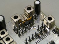
I attached some pictures of this balanced twin-crystal masterclock.
Could you please address what was your reasoning in deciding not to include a comparator immediately after the oscillator buffer J-FETs?
Comparators add significant propagation delay and resulting jitter. The reference voltage is also very critical, the slightest noise on this voltage will translate to jitter at the comparator output. The comparator also places a substantial amount of extra components in the clock signal path.
I designed the masterclock so it outputs approx. 10Vpp with relative fast transients, this way I can leave out comparator and related problems. The transients are still fast enough for accurate triggering of connected circuits. The signal at the crystals is sine wave shaped with up to 50Vpp amplitude at 4V power supply. I use chokes to boost signal amplitude and provide high impedance between oscillator output and GND.
Similar to audio signal path, it's best to place minimum amount of components in the clock signal path as every extra component reduces resolution as a result of their typical properties. The audible results are increased grain (even audible distortion at specific frequencies) and reduced detail.
Since my masterclocks outputs approx +/-5V I need to use fast rectifiers / attenuators to match digital input specs of connected CMOS circuits.
Constructing a low jitter masterclock is difficult, but when connecting clock loads things get much worse.
Connected clock loads will inter-act (despite clock buffer that also introduces problems). So best would be using a separate clock buffer for every connected load. This in turn would place too high load on the masterclock.
Then there is the issue that an un-buffered output offers higher resolution than a buffered output, but the buffer is required to prevent degrading with connected loads.
I attempted to solve this with the latest balanced twin-crystal masterclock. This masterclock has two outputs, so I connected the bit reclocker (3pF load) to one output and the SD-transport to the other (no clock buffers required). Measurements showed that both outputs are "isolated" so inter-action between both clock loads is minimal. Then there are the advantages of a balanced circuit (PSRR). The balanced oscillator runs on two closely matched 2SK170 JFETs (very low noise and high gain). Clock buffers could be left out because there is only a single clock load (approx. 3pF) on each output. This offers maximum detail and lowest grain.
I used 2 crystals to achieve a clock signal very close to 11.2896 MHz without using a trimmer. The power dissipation in each crystal is also reduced this way.
In order to benefit from the increased masterclock performance, the circuit must be fully screened.
I attached some pictures of this balanced twin-crystal masterclock.
Attachments
Thanks for the reply
Hi Ken Newton,
I attempted to solve this with the latest balanced twin-crystal masterclock. This masterclock has two outputs, so I connected the bit reclocker (3pF load) to one output and the SD-transport to the other (no clock buffers required).
Hi John,
Thank you for that reply.
1. Can I safely assume that your new balanced oscillator design has the crystals connected in series and so the pair differentially drive the two JFETs in locked anti-phase?
Regards,
Ken
Hi Ken Newton,
That's correct.
The oscillator consists of two 11.2896 High-Q crystals, two matched low noise audio FETs, two 150uH hybrid chokes, and two 1 M Ohm resistors from gate to GND. Output signal is rectified using RF Schottky diode and 330R load resistor to GND.
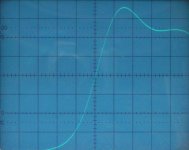
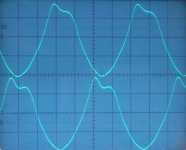
I attached oscillogram of signal at JFET source (1V/div, 5ns/div). The signal swings around GND (goes positive and negative) so rectifier is required to match connected CMOS load properties.
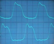
Second oscillogram shows both phase-shifted rectified output signals. Differences in waveform are caused by using two different probes (one of my Tektronix probes broke). Both probes were correctly calibrated using the Hameg scope built-in calibrator.
Positive transient rise time equals approx. 5ns. Synchronous reclockers and SD-transport trigger on this positive transient. Oscillogram shows output signals with 3pF clock loads and 15pF scope probe connected. So the scope probe introduces approx. 5 times higher load than the actual clock loads. This shows one of the limitations of measurements, and why circuits can perform different with or without probe attached. While measuring I also introduce a ground loop as both scope and oscillator are mains-powered.
Third oscillogram shows the balanced output signals before the rectifiers. The rectifiers basically "chop-off" the part of the clock signal that goes negative.
1. Can I safely assume that your new balanced oscillator design has the crystals connected in series and so the pair differentially drive the two JFETs in locked anti-phase?
That's correct.
The oscillator consists of two 11.2896 High-Q crystals, two matched low noise audio FETs, two 150uH hybrid chokes, and two 1 M Ohm resistors from gate to GND. Output signal is rectified using RF Schottky diode and 330R load resistor to GND.
I attached oscillogram of signal at JFET source (1V/div, 5ns/div). The signal swings around GND (goes positive and negative) so rectifier is required to match connected CMOS load properties.
Second oscillogram shows both phase-shifted rectified output signals. Differences in waveform are caused by using two different probes (one of my Tektronix probes broke). Both probes were correctly calibrated using the Hameg scope built-in calibrator.
Positive transient rise time equals approx. 5ns. Synchronous reclockers and SD-transport trigger on this positive transient. Oscillogram shows output signals with 3pF clock loads and 15pF scope probe connected. So the scope probe introduces approx. 5 times higher load than the actual clock loads. This shows one of the limitations of measurements, and why circuits can perform different with or without probe attached. While measuring I also introduce a ground loop as both scope and oscillator are mains-powered.
Third oscillogram shows the balanced output signals before the rectifiers. The rectifiers basically "chop-off" the part of the clock signal that goes negative.
Attachments
Then there are the advantages of a balanced circuit (PSRR).
Yes, but only if both outputs are combined by another circuit, here most likely a comparator.
That comparator finally increases the PSSR by rejecting common mode PS induced noise.
I use balanced oscillator, balanced comparator and balanced flipflop.
And after that balanced DAC chips.
I'm selling my Thomas ultimate TDA1541A kit (v2). If anybody is interested check the classified section.
Yes, but only if both outputs are combined by another circuit, here most likely a comparator.
That comparator finally increases the PSSR by rejecting common mode PS induced noise.
I use balanced oscillator, balanced comparator and balanced flipflop.
And after that balanced DAC chips.
Bernard, will you please so kind to share your balanced schematics ?!
Thanks in advance.
Regards,
Onno
Bernard, will you please so kind to share your balanced schematics ?!
I have not drawn an updated complete schematic yet.
Oszillator part:
http://www.diyaudio.com/forums/digital-source/154401-differential-clock-2.html#post1998528
Comparator part with 2 x cmos output for cmos flipflop and slaved transport:
http://www.diyaudio.com/forums/digital-source/154401-differential-clock-4.html#post2003972
If you want to use a balanced ECL flipflop for reclocking, remove one part of the mc10125.
Best read the whole thread.
Hi John,
I am using one of your DI8M boards with 4 x TDA1541 chips and would like to try out the latest DEM injection scheme, single flip flop reclocking, attenuation and also the DJA circuit.
After studying the Schematics that you recently posted of your MK3 DAC I can see a number of different ways of updating the timing control on my DAC, but would like to know what would be the best way forward.
I am using your Tracker module with the SPDIF receiver and also direct I2S from a slaved Squeezebox.
can I get away with one DEM reclock circuit and DJA to drive all 4 DACs? I notice that the BCK signal for your MK3 DAC is also taken from part of the DEM clock circuit - can I do the same for all 4 of my DACs?
would it be beneficial to reclock and attenuate the WS and DATA lines on each TDA chip with a flip flop placed right next to each input on the DAC and using the BCK as a control?
I know that you will be looking at updating the DI8M DAC and will be including some of the advances that are seen in the MK3, but I would really like to try out some of the above and appreciate your thoughts.
Brad
Hi Builder Brad,
Final balanced DEM synchronizer circuit is driven by Q and /Q outputs (1.4112 MHz)of the bit reclocker. It has 2 x Schottky diode > 2 x 12K > 2 x 2K2 to -15V.
Final clocking scheme:
Balanced Masterclock Q output > Bit reclocker (clock load #1).
Balanced Masterclock /Q output > SD-transport (clock load #2).
Bit reclocker Q and /Q outputs > I2S attenuator > BCK.
Bit reclocker Q and /Q outputs > DEM synchronizer > DEM and /DEM.
Bit reclocker /Q output > DATA and WS reclockers.
Propagation delay between masterclock Q output and and BCK, approx. 800ps.
When using 4 DAC chips, construct 4 separate DEM synchronizer circuits and connect all to the bit reclocker.
Bit reclocker attenuated output can drive 4 DAC chip BCK inputs. Data and WS reclockers can also drive 4 DAC chips Data and WS inputs.
The latest TDA1541A version is the MK4, it is quite different from the schematics of the MK3.
I think I2S with shortest possible interconnects between source and DAC performs best by far. SPDIF is nice for driving an external DAC but for high performance audio I think it's definitely a dead end.
It's already extremely difficult to maintain low jitter and interference levels when using one masterclock and a virtually perfect digital audio source that is located close to the DAC chip and masterclock.
Data and WS signals need to have lowest possible jitter and fast transients just like the bit clock. Try to minimize the amount of flip-flops to absolute minimum, that's basically one for each I2S signal.
I have to redesign the DI8 timing module to accept 32 bits / frame before I can do some more tests in combination with the SD-transport.
Right now I am redesigning my bridge power amps as they couldn't keep up with MK4 performance. The ON resistance of 2SK1058 and 2SJ62 MOSFETs was too high (lateral FETs), the bridge output doubles this ON resistance.
Now I built a FET circlotron amp with similar input and driver circuit as with the bridge power amp, but with 2 x 2SK1530 in the circlotron power stage. It uses a floating stabilized power supply for the driver stage and two more floating power supplies for the circlotron power stage. Each power amp has 6 FETs in total, 1 x 2SK389 (dual), 1 x 2SJ109 (dual) and 2 x 2SK1530.
The advantages of the circlotron are same type (matched) power FETs for both, positive and negative signal half. Power section is isolated from the driver section. Bridge output using only 2 instead of 4 power FETs, lowest possible input capacitance of the power stage (700 ... 900pF) since only 1 FET needs to be driven by each output of the balanced driver.
Bias is set by varying bias current in the input stage, and a compensation diode / transistor to prevent thermal runaway.
I am using one of your DI8M boards with 4 x TDA1541 chips and would like to try out the latest DEM injection scheme, single flip flop reclocking, attenuation and also the DJA circuit.
Final balanced DEM synchronizer circuit is driven by Q and /Q outputs (1.4112 MHz)of the bit reclocker. It has 2 x Schottky diode > 2 x 12K > 2 x 2K2 to -15V.
Final clocking scheme:
Balanced Masterclock Q output > Bit reclocker (clock load #1).
Balanced Masterclock /Q output > SD-transport (clock load #2).
Bit reclocker Q and /Q outputs > I2S attenuator > BCK.
Bit reclocker Q and /Q outputs > DEM synchronizer > DEM and /DEM.
Bit reclocker /Q output > DATA and WS reclockers.
Propagation delay between masterclock Q output and and BCK, approx. 800ps.
When using 4 DAC chips, construct 4 separate DEM synchronizer circuits and connect all to the bit reclocker.
Bit reclocker attenuated output can drive 4 DAC chip BCK inputs. Data and WS reclockers can also drive 4 DAC chips Data and WS inputs.
After studying the Schematics that you recently posted of your MK3 DAC I can see a number of different ways of updating the timing control on my DAC, but would like to know what would be the best way forward.
The latest TDA1541A version is the MK4, it is quite different from the schematics of the MK3.
I am using your Tracker module with the SPDIF receiver and also direct I2S from a slaved Squeezebox.
I think I2S with shortest possible interconnects between source and DAC performs best by far. SPDIF is nice for driving an external DAC but for high performance audio I think it's definitely a dead end.
It's already extremely difficult to maintain low jitter and interference levels when using one masterclock and a virtually perfect digital audio source that is located close to the DAC chip and masterclock.
would it be beneficial to reclock and attenuate the WS and DATA lines on each TDA chip with a flip flop placed right next to each input on the DAC and using the BCK as a control?
Data and WS signals need to have lowest possible jitter and fast transients just like the bit clock. Try to minimize the amount of flip-flops to absolute minimum, that's basically one for each I2S signal.
I know that you will be looking at updating the DI8M DAC and will be including some of the advances that are seen in the MK3, but I would really like to try out some of the above and appreciate your thoughts.
I have to redesign the DI8 timing module to accept 32 bits / frame before I can do some more tests in combination with the SD-transport.
Right now I am redesigning my bridge power amps as they couldn't keep up with MK4 performance. The ON resistance of 2SK1058 and 2SJ62 MOSFETs was too high (lateral FETs), the bridge output doubles this ON resistance.
Now I built a FET circlotron amp with similar input and driver circuit as with the bridge power amp, but with 2 x 2SK1530 in the circlotron power stage. It uses a floating stabilized power supply for the driver stage and two more floating power supplies for the circlotron power stage. Each power amp has 6 FETs in total, 1 x 2SK389 (dual), 1 x 2SJ109 (dual) and 2 x 2SK1530.
The advantages of the circlotron are same type (matched) power FETs for both, positive and negative signal half. Power section is isolated from the driver section. Bridge output using only 2 instead of 4 power FETs, lowest possible input capacitance of the power stage (700 ... 900pF) since only 1 FET needs to be driven by each output of the balanced driver.
Bias is set by varying bias current in the input stage, and a compensation diode / transistor to prevent thermal runaway.
Now I built a FET circlotron amp
Circlotron are sexy 🙂
Do you use "gate stoppers" around 500R, by chance 😉
I plan to use honeycombs on my next FET amps 😎
Good luck.
M.
Thank-you for the detailed reply John.
I am now working off of what I believe are the latest DEM and attenuation circuits that you posted on the 18/8.
I am not able to find a flip flop ic that matches the 74AU1G74 chip shown in your Schematics. I am about to order some other items with digikey UK can you recomend an flip flop that is suitable for the DEM and reclock circuits.
Not sure how I will be able to avoid lots of flip flops on the DATA and WS signals as they are all frame shifted by the timming module on the D8M, so it looks like I will need to reclock each of those lines to each DAC. BCK will be ok to drive all chips though,.
Brad
Hi maxlorenz,
I am experimenting with circlotrons because I need a bridge amplifier with only 1 JFET in the power signal path and closely matched JFETs (same type) for both positive and negative signal half. I use 120R gate resistors in the prototype setup because of the long wires running to the powerFET gates.
I plan to use wirewound resistors (Tyco / Rhopoint) for the higher values up to 100K and Honeycomb / Mobius for the lower values up to 1K. Exception are the bias and balance setting trimmers.
I have been testing the new TDA1541A-MK4 DAC module for some weeks now. The sound quality of this DAC differs significantly from the previous designs with the 4-crystal clock. First thing one notices is the relaxed sound, all detail and speed are still there, but the relation to the music is much more natural. I am testing the DAC on mains power at the moment.
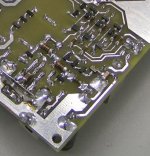
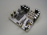
First picture shows the component side, un-interrupted ground plane is used. I use two JFETs in parallel (lower noise) for each channel. I/V conversion is passive (500R Mobius / Honeycomb resistors). Bias resistors are 5K wire wound from Rhopoint / Tyco. I removed the active buffer and use +5V as signal reference. I tap the output signal directly from the I/V resistor, excluding the +5V power supply from the direct signal path. This results in fewest components in the signal path (one I/V resistor and one hybrid coupling cap). The TDA1541A (1998) is cryo-treated.
All chokes are screened now in order to minimize the effects of EMI. Heart of the circuit is a twin-crystal balanced masterclock, based on the 4-crystal masterclock concept. By connecting only a single, low capacitance clock load to each of the outputs of the balanced masterclock, clock buffers (and extra propagation delay / jitter) could be avoided.
Some ferrite beads are changed to different types now (not shown on this photograph) in order to further improve performance. Masterclock and bit reclocker are now powered through a 12th order low pass filter.
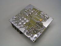
Second picture shows solder side. Here we can see decoupling caps, 3 synchronous reclockers (BCK, WS, and DATA), diode resistor I2S attenuators, and diodes for reducing power supply voltage to approx. 2.5V for the synchronous reclockers. DEM circuit consists of balanced DC-coupled circuit with BAT17, 12K and 2K2. It's driven directly from the bit reclocker (1.4112 MHz DEM clock). I2S and clock Wiring is kept as short as possible.
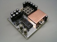
Third picture shows the MK4 with an experimental copper screen around masterclock and synchronous reclockers. I plan to replace this screen with a tinned metal screen.
Circlotron are sexy
Do you use "gate stoppers" around 500R, by chance
I plan to use honeycombs on my next FET amps
I am experimenting with circlotrons because I need a bridge amplifier with only 1 JFET in the power signal path and closely matched JFETs (same type) for both positive and negative signal half. I use 120R gate resistors in the prototype setup because of the long wires running to the powerFET gates.
I plan to use wirewound resistors (Tyco / Rhopoint) for the higher values up to 100K and Honeycomb / Mobius for the lower values up to 1K. Exception are the bias and balance setting trimmers.
I have been testing the new TDA1541A-MK4 DAC module for some weeks now. The sound quality of this DAC differs significantly from the previous designs with the 4-crystal clock. First thing one notices is the relaxed sound, all detail and speed are still there, but the relation to the music is much more natural. I am testing the DAC on mains power at the moment.
First picture shows the component side, un-interrupted ground plane is used. I use two JFETs in parallel (lower noise) for each channel. I/V conversion is passive (500R Mobius / Honeycomb resistors). Bias resistors are 5K wire wound from Rhopoint / Tyco. I removed the active buffer and use +5V as signal reference. I tap the output signal directly from the I/V resistor, excluding the +5V power supply from the direct signal path. This results in fewest components in the signal path (one I/V resistor and one hybrid coupling cap). The TDA1541A (1998) is cryo-treated.
All chokes are screened now in order to minimize the effects of EMI. Heart of the circuit is a twin-crystal balanced masterclock, based on the 4-crystal masterclock concept. By connecting only a single, low capacitance clock load to each of the outputs of the balanced masterclock, clock buffers (and extra propagation delay / jitter) could be avoided.
Some ferrite beads are changed to different types now (not shown on this photograph) in order to further improve performance. Masterclock and bit reclocker are now powered through a 12th order low pass filter.
Second picture shows solder side. Here we can see decoupling caps, 3 synchronous reclockers (BCK, WS, and DATA), diode resistor I2S attenuators, and diodes for reducing power supply voltage to approx. 2.5V for the synchronous reclockers. DEM circuit consists of balanced DC-coupled circuit with BAT17, 12K and 2K2. It's driven directly from the bit reclocker (1.4112 MHz DEM clock). I2S and clock Wiring is kept as short as possible.
Third picture shows the MK4 with an experimental copper screen around masterclock and synchronous reclockers. I plan to replace this screen with a tinned metal screen.
Attachments
Hi Builder Brad,
Final DEM injector uses 2 x BAT17 Schottky diodes, 2 x 12K series resistors and 2 x 2K2 resistors between pin 16 and -15V and pin 17 and -15V. It's a balanced DC-coupled synchronizer running at 1.4112 MHz. I tap the balanced DEM clock from the synchronous bit reclocker Q and /Q outputs. Decoupling caps are 47nF / 16V SMD PPS and are mounted underneath the TDA1541A for shortest possible return path.
I may have missed a faster available CMOS D flip-flop, but the 74AU1G74 is the one with the lowest propagation delay I could find. D flip-flops with higher propagation delay I tested so far introduce clearly audible degrading effect (grain / distortion). The 74HC series have too high propagation delay for these demanding applications.
Other problem is the physical size of the chip. Smaller chips allow for shorter wiring and more efficient power supply decoupling. It's also very important to use a single flip-flop / package in order to minimize interference between multiple flip-flops. I use power supply LC filters on every single flip-flop.
The shift registers for DATA and WS already reclock these signals, but due to shift register properties, jitter and interference levels are still too high.
So you will need at least 9 synchronous reclockers, BCK, DATA (4x) and WS (4x). This is another reason why I returned to a single DAC chip solution. I only require 3 synchronous reclockers now.
Thank-you for the detailed reply John.
I am now working off of what I believe are the latest DEM and attenuation circuits that you posted on the 18/8.
I am not able to find a flip flop ic that matches the 74AU1G74 chip shown in your Schematics. I am about to order some other items with digikey UK can you recomend an flip flop that is suitable for the DEM and reclock circuits.
Final DEM injector uses 2 x BAT17 Schottky diodes, 2 x 12K series resistors and 2 x 2K2 resistors between pin 16 and -15V and pin 17 and -15V. It's a balanced DC-coupled synchronizer running at 1.4112 MHz. I tap the balanced DEM clock from the synchronous bit reclocker Q and /Q outputs. Decoupling caps are 47nF / 16V SMD PPS and are mounted underneath the TDA1541A for shortest possible return path.
I may have missed a faster available CMOS D flip-flop, but the 74AU1G74 is the one with the lowest propagation delay I could find. D flip-flops with higher propagation delay I tested so far introduce clearly audible degrading effect (grain / distortion). The 74HC series have too high propagation delay for these demanding applications.
Other problem is the physical size of the chip. Smaller chips allow for shorter wiring and more efficient power supply decoupling. It's also very important to use a single flip-flop / package in order to minimize interference between multiple flip-flops. I use power supply LC filters on every single flip-flop.
Not sure how I will be able to avoid lots of flip flops on the DATA and WS signals as they are all frame shifted by the timming module on the D8M, so it looks like I will need to reclock each of those lines to each DAC. BCK will be ok to drive all chips though,.
The shift registers for DATA and WS already reclock these signals, but due to shift register properties, jitter and interference levels are still too high.
So you will need at least 9 synchronous reclockers, BCK, DATA (4x) and WS (4x). This is another reason why I returned to a single DAC chip solution. I only require 3 synchronous reclockers now.
- Home
- Source & Line
- Digital Line Level
- Building the ultimate NOS DAC using TDA1541A