Thank you
With Mark's help, thank you, I/we have dealt to my turn-on thump and turn-off pop.
I installed Mark's suggested new/altered mute circuit components and I'm a happy camper.
This is one sweet sounding amp.
t
With Mark's help, thank you, I/we have dealt to my turn-on thump and turn-off pop.
I installed Mark's suggested new/altered mute circuit components and I'm a happy camper.
This is one sweet sounding amp.
t
can l substitute LM 4562 by LM 49720 as l have it already in hand ?
They are the same parts, just a different numbering system.
And no, it's not a good idea to sub a bipolar input opamp for the servo. A good old tl071 would work in this context though if you can't get an opa134.
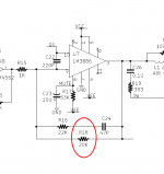
Here is the pencil and paper method of gain calculation. It gives answers that are about 5% below yours. More importantly, pencil+paper matches the gain number Bob Cordell wrote in his book: page 686 of the 2nd edition, page 541 of the 1st edition.
_
Thanks for that.
The schematic shows R6 as 47k and R7 as 470. You used different values for the calculation. Any reason for this that I should be aware of before the build.
Referring to Bob's official schematic in post #9 of this thread, gain is equal to (R11 / R9).
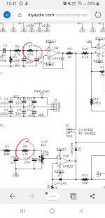
values of 78L15 and 79L15 bypass caps
I notice that C10, 15, 16 and C19,20, 21 are all in parallel with a value of 100NF.
any audible differences if l replace one or two caps with other values such as 200nf ?
I notice that C10, 15, 16 and C19,20, 21 are all in parallel with a value of 100NF.
any audible differences if l replace one or two caps with other values such as 200nf ?
Each of the three DIP-8 integrated circuits has its own dedicated pair of supply bypass capacitors. On the printed circuit board, these caps are immediately adjacent to the supply pins of the DIP, for tight coupling and effective bypassing. However, on the schematic, these caps have been moved out of the way, to make the signal paths easier to read (less cluttered).
"U4" (the input receiver chip) has C10 and C19
"U5" (the Klever Klipper chip) has C16 and C21
"U8" (the DC servo chip) has C15 and C20
You can verify this when you've got a PCB in your hands.
As far as I'm aware, nobody has built a set of four Super Gainclone boards, two with C10=C15=C16=C19=C20=C21 = 100nF, and two more boards with different capacitance values in those positions, then listened to the resulting pair of stereo amplifiers. So "any audible differences" is not a hypothesis that's been tested, at least not so far.
Remember that it's your D.I.Y. project and you can build it any way you like. It seems like a fairly low risk experiment to try different values of bypass capacitor(s) and discover whether you enjoy the results. It might be a lot of fun!
Mark,
thank you for the reply.
I have the pcb in hand.
i will go ahead and solder 1206 smd X7R capacitors next to the DIP sockets for bypass.
I am trying to use up old stocks of parts to make way for more new projects.
thank you for the reply.
I have the pcb in hand.
i will go ahead and solder 1206 smd X7R capacitors next to the DIP sockets for bypass.
I am trying to use up old stocks of parts to make way for more new projects.
Sure, give it a try! You may want to also build an experimental control using the film (not ceramic X7R) capacitors called for in the Detailed Parts List. Just to find out whether there are, or are not, "any audible differences". Have fun!
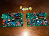
In November I sold (at my cost) the excess boards I hadn't used myself, from the initial prototyping run at the PCB fab. There weren't a lot of PCBs; all were gone after only eleven orders.
Then in December I launched a Group Buy, for much greater quantities. This time there were many more buyers, and everyone got a nice volume discount. The orders have been placed, the money has been collected, and now we're waiting for the GB boards to ship from China to California.
Then in December I launched a Group Buy, for much greater quantities. This time there were many more buyers, and everyone got a nice volume discount. The orders have been placed, the money has been collected, and now we're waiting for the GB boards to ship from China to California.
value of C23, mute pin capacitor
l notice that the datasheet application circuit uses 100 uf instead of 10 uf in the supergainclone circuit .
i am learning electronic and in this circuit if l use 100uf, there will be a switch off thump on powering off because the power supply to the DIP op amp collapsed earlier .
Am l correct with the reasoning?
Bob Cordell's design is shown in post #9. It has ten microfarads on the LM3886 MUTE pin. The schematic for this Super Gain Clone PCB (in post #1) also has ten microfarads on the LM3886 MUTE pin. I recommend that you connect ten microfarads to the MUTE pin.
Despite this recommendation, if you still want to experiment, please go right ahead! It's okay to deviate from the recommended values, as long as you remember you are taking a risk. In snow skiing it's called "off piste" -- you have chosen to ski where there is no marked trail -- and if you fall down & get hurt, nobody will find your dead frozen body for several days. This is D.I.Y. after all, emphasis on the Y. Do what You want to do and have some fun! Play with whatever "knobs" you like.
There are other, non-Bob-Cordell designs for LM3886 boards "out there" which install a Zener diode in the mute circuit, supposedly for extra margin of safety. (Bob's Super Gain Clone design has no Zener diode in the mute circuit). An early, early builder of this PCB has deviated from the official schematic and installed a Zener diode (not on the schematic!) in her/his Mute circuit of her/his board. I understand that s/he is happy with the result.
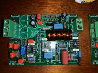
Please have a look at the "silk screen" lettering on the top side of the PCB. Its purpose is to help you know which layout footprint corresponds to a certain schematic component.
You can also treat the question as a recreational puzzle: figure out what goes where by gathering all the clues and then following them to a conclusion. For example ...
The schematic says that one of R18's legs is connected to LM3886 pin 3, and its other leg is connected to LM3886 pin 9.
Therefore we expect to find R18 somewhere close the LM3886. And indeed it is close! R18 is the very first component below the LM3886. See plot below.
_
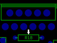
Attachments
- Home
- Amplifiers
- Chip Amps
- Bob Cordell's Super Gain Clone PCB (LM3886) and a stripped-down version: Compact3886