I have been swapping drain & source of JFETs for years.
Absolutely no issue at all.
Applies to all small signal JFETs I know of, not only Toshibas.
Although I have not tried with LU1014 or Semisouth.
No real need in those cases.
It helps to understand some semiconductor physics.
Cheers,
Patrick
Absolutely no issue at all.
Applies to all small signal JFETs I know of, not only Toshibas.
Although I have not tried with LU1014 or Semisouth.
No real need in those cases.
It helps to understand some semiconductor physics.
Cheers,
Patrick
Last edited:
> The idea is to make a B1 R1, not R2.
The purpose of his drain resistors is to measure current / for debug.
For the lower half (CCS), it does not matter whether it is connected to the drain or the source.
Patrick
The purpose of his drain resistors is to measure current / for debug.
For the lower half (CCS), it does not matter whether it is connected to the drain or the source.
Patrick
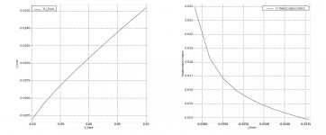
250x 2SK2145GR wired as source follower at 4mA Idss per FET would make :
Idss ~1A
Transconductance 3S (Zout 0.3R)
Crss ~750pF
Compared with say 2SK1530 at 1A bias
Transconductance ~2S (Zout 1R)
Crss ~100pF
Compared with SJEP120R100 at 1A bias
Transconductance ~5S (Zout 0.2R)
Crss ~100pF
None of them has low enough Zout without NFB.
Both Toshiba's have positive tempco which needs to be dealth with.
And you will need a low-Z gain stage to drive the 2SK2145's.
Cheers,
Patrick
Thank you, Patrick. I appreciate your advice based on experience.
The attraction is a completely JFET power amp using devices in production. The output impedance appears to be low enough for Mr. Pass to drive various speakers and he approves of the sound. That is enough reason for me to try one or more variants.
The versions I am working on are using devices in stock at the large reputable distributors.
I will look into adding driver buffer(s) on board similar to what Mr. Pass did.
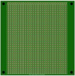
At the moment, the device count for the massive B1 is 500 pcs of 2SK2145 per board. I may increase that to 1,000. The board size will be within allowable dimensions at the fab I use.
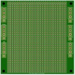
I may try a 100mm x 100mm SMT version as a trial run.
The attraction is a completely JFET power amp using devices in production. The output impedance appears to be low enough for Mr. Pass to drive various speakers and he approves of the sound. That is enough reason for me to try one or more variants.
The versions I am working on are using devices in stock at the large reputable distributors.
I will look into adding driver buffer(s) on board similar to what Mr. Pass did.
At the moment, the device count for the massive B1 is 500 pcs of 2SK2145 per board. I may increase that to 1,000. The board size will be within allowable dimensions at the fab I use.
I may try a 100mm x 100mm SMT version as a trial run.

Then, can I use J113+J175 instead of 2sk170+j74?
Same resistors as original Beast?
Matching needed?
J113 and J175 are stock and cheap parts. Good!
Same resistors as original Beast?
Matching needed?
J113 and J175 are stock and cheap parts. Good!
Then, can I use J113+J175 instead of 2sk170+j74?
Same resistors as original Beast?
Matching needed?
J113 and J175 are stock and cheap parts. Good!
The pin-out for J113/J175 is different than K170/J74.
Idss of J113/J175 is 2x or more than K170/J74.
You do not need to match pairs. You can match the total groups. For example, you may need 50 pcs of J175 and 40 pcs of J113 to achieve minimum output offset voltage. That is why I am designing with drain resistors. You can remove a resistor to disable a JFET.
The output impedance of the amplifier will be larger than K170/J74 Beast.
You can sort the JFETs easily with a plug in proto board and a power supply and a DMM. That is what I do. I make a row of receptacles with labels 21mA, 22mA, 23 mA, etc.
You can make a spreadsheet with quantities of each Idss container. Then group them all for a close match of Idss for N and for P.
I allow the JFETs to warm up until they have a stable Idss reading. The temp coefficient makes the parts change Idss 10% to 20% from cold to hot.
Woofertester, thank you for so long and detailed answer. Many things are clearer now.
I have to: classify jfets, check wattage/dissipation, put bigger resistors, change pinouts, make some boards and mount two amps.
I think it worths trying, even it's at my limit. We're confinated now in Spain, boredom is my friend. 😉
Again thank you
I have to: classify jfets, check wattage/dissipation, put bigger resistors, change pinouts, make some boards and mount two amps.
I think it worths trying, even it's at my limit. We're confinated now in Spain, boredom is my friend. 😉
Again thank you
Woofertester, thank you for so long and detailed answer. Many things are clearer now.
I have to: classify jfets, check wattage/dissipation, put bigger resistors, change pinouts, make some boards and mount two amps.
I think it worths trying, even it's at my limit. We're confinated now in Spain, boredom is my friend. 😉
Again thank you
I hope this helps relieve some boredom for you.
Woofertester, thank you for so long and detailed answer. Many things are clearer now.
I have to: classify jfets, check wattage/dissipation, put bigger resistors, change pinouts, make some boards and mount two amps.
I think it worths trying, even it's at my limit. We're confinated now in Spain, boredom is my friend. 😉
Again thank you
Bigger resistors will not solve a power dissipation problem. The circuit will have to be redesigned to add source resistors for local degeneration. This will lower bias current and may increase output resistance.
For now, just live with the J175 operating its power limit.
I wonder if anyone considered putting their beasts in a tank and filling it up with fluorinert and an aquarium pump to circulate, one of those neat waterfalls for cooling just like Cray did.
HAM Geezers did that with their melting 807s and 6L6 ..... bucket of oil ......
why one should the same with eeny tiny weeny JFets?
if you push them in enormous current region , byebye any linearity
why one should the same with eeny tiny weeny JFets?
if you push them in enormous current region , byebye any linearity
if you push them in enormous current region , byebye any linearity
When I have a pcb populated, I will post some scope shots. If linearity is bad, it should be visible on the scope.
enormous current region means - above Idss ....... gate going positive ref. to source
I can't see that your pcbs are made to accommodate that (and they shouldn't be)
I can't see that your pcbs are made to accommodate that (and they shouldn't be)
Below is the basic schematic for a CCS beast cell. R3 is just a gate resistor. Any value from 200 to 1k ohms will fine. Nelson's micro-beast uses 470 ohms for R3.
For good linearity from the J113 jfet, Nelson's bias resistor, R2, is 47 ohms for 10 to 15 milliwatts dissipation per J113. Even at that dissipation, I can't keep my fingers on the jfets for more that 10 seconds. So heat dissipation needs to be taken into account.
Lastly, R1 is 47 ohms. One drawback of the J113 jfet is Idss values range from 7 to 30. So matching J113s is important.

- Home
- Amplifiers
- Pass Labs
- Beast with 1000 JFETs redux?