Ok.....sounds good and very interesting.
Can just JFETs from "the box" be used without any matching?
Can just JFETs from "the box" be used without any matching?
I believe GR range with cleverly sizes source resistor will enable use of JFets without selection
1000pcs?? Vasting precious discrete jfets, they are all ready disappearing...Here is what I think is the "optimal" layout for the buffer. It consumes 0.2 inches^2. It is two of the 2SK2145
This is 4 transistors comprising two parallel buffers.
The NP original Beast 14" x 21" board costs double extra because of large size and is larger than needed for the SMT version.
The plan is to make a 10" x 12" board with room at the top and bottom for power and signal terminal strips.
1000 pcs of 2SK2145 should fit on one side. It will be 1000 B1 buffers in parallel.
Using the Y grade of the 2SK2145, it should be possible to run at + / - 15V and not have power dissipation problems at each device.
Bias current will be at least 1.2A, probably closer to 2A.
How many "Beast" projects are currently under development that will be available for some kind of DIY?
Is there also a NP-project that could be available via the DiyStore?
Is there also a NP-project that could be available via the DiyStore?
1000pcs?? Vasting precious discrete jfets, they are all ready disappearing...
No. Not at all. I am using JFETs that I buy from Mouser/Digikey/Rochester.
Any hobbyist can buy these JFETs.
How many "Beast" projects are currently under development that will be available for some kind of DIY?
Is there also a NP-project that could be available via the DiyStore?
I do not speak for NP or the DIY Audio Store. Just doing my own version with what I know and what I can buy from distributors.
I believe GR range with cleverly sizes source resistor will enable use of JFets without selection
No source resistors for me. I look at that as a waste of gm. My opinion could change if facts convince me otherwise.
My plan for matching and adjusting output offset is to remove one or more drain resistors from the offending 1/2 of the buffer. The design is such that a soldering iron carefully used can make it happen.
The plan is to use Y grade 2SK2145.
Last edited:
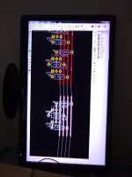
The first through-hole boards arrived and it was a disappointment due to solder footprint of the transistors. Almost impossible to solder for me.
Rev 2 of the through-hole board is now in layout. Resorted to turning my screen sideways. This is so much better for placing and aligning cells in columns.
I think that the basic cell in now improved as well. Learning how to orient and space footprints better.
My goal is ease of bus routing rather than nice neat columns of parts.
The basic layout fits on one side of the board. Back side copper for routing the buses between columns.
Attachments
Last edited:
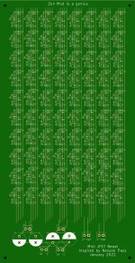
Mini Beast V2 board
160mm x 310mm double sided
I am pleased with the new cell layout for stacking in columns.
The specifics of getting these to move and stack is tedious and could do with some automation.
There are ostensibly plugins to help Kicad and they garble the cell so no help from the "place footprints" plugin. The "replicate layout" plugin is immensely helpful.
This was about two full days of layout work. Quite a few more days to learn enough to know how to spend the two days on this layout.
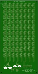
There appear to be connection problems and wrong traces on the filter caps and PS connectors.
Also on the Vin and Vout connectors. NP name is spelled wrong.
Also on the Vin and Vout connectors. NP name is spelled wrong.
Last edited:
For example, are there not traces shorting together each of the six connectors' 2 pins?
That would be a net error, not a DRC error.
That would be a net error, not a DRC error.
Last edited:
No. Not at all. I am using JFETs that I buy from Mouser/Digikey/Rochester.
Any hobbyist can buy these JFETs.
I now, I wanted to say that you could make hundreds of different circuits with all these jfets... Is there a real advantage of this concept except "because I can"? 🙂
The DC filtering and current distribution need attention.
Wouldn't it be better to use a layer for each DC rail, and then short via to where's needed??
Wouldn't it be better to use a layer for each DC rail, and then short via to where's needed??
I now, I wanted to say that you could make hundreds of different circuits with all these jfets... Is there a real advantage of this concept except "because I can"? 🙂
The JFETs are not as low noise as 2SK170/2SJ74 and so all of the large voltage gain applications are not desirable (for me).
The massively parallel JFET follower is lower distortion than a MOSFET or a BJT and the distortion signature lacks the higher order harmonics that you would get with a BJT. The circuit is zero feedback. Read Nelson's article.
High power complementary JFETs do not exist. So, rolling your own from small signal JFETs is a solution.
If you read Nelson's article, his conclusion is that the Beast is worthy of building and listening to. That is the reason I am building these versions, to listen to and use.
Another attraction is that there is no heatsink to deal with. A very big plus for me.
For example, are there not traces shorting together each of the six connectors' 2 pins?
That would be a net error, not a DRC error.
The problem is that I did not label every pin. Now it should be clear. I also added a GND terminal block between the signal terminal blocks.
Top view and bottom view attached.
Attachments

The DC filtering and current distribution need attention.
Wouldn't it be better to use a layer for each DC rail, and then short via to where's needed??
Good points. Just learning 2-layer layout now. a 4-layer version would be a refinement/upgrade.
I can measure the traces and quantify the resistance of the tracks. If the tracks are high resistance compared to the impedance of the JFETs, then your idea would be called for.
Another attraction is that there is no heatsink to deal with. A very big plus for me.
No heatsink is a big plus for me too. And the amplifier is scalable.
It's a very interesting project.
- Home
- Amplifiers
- Pass Labs
- Beast with 1000 JFETs redux?