How much ripple do you want?
https://ocw.mit.edu/courses/electri...-spring-2007/study-materials/ripple_volts.pdf
https://ocw.mit.edu/courses/electri...-spring-2007/study-materials/ripple_volts.pdf
JFETs are trickling in. Measurements are happening.
My thinking is that + / - 5V rails with a bias of 250mA should work for headphones and flea power speakers. My intention is that the current gain will be at least 250mA / V.
Discussion is welcome.
I have several flea power speakers. And I'm very interested in your project, waiting first results. I can help building prototipe, if needed.
A 5w microBeast would be very nice.
Victor
PCB Preview. Ordered some. We shall see how it works
Good job woofertester. 🙂
Member
Joined 2009
Paid Member
Maybe somebody would offer a Group Buy, surface mount parts, built to a finished state by a subcontractor using industry standard pick n place machine for completed PCBA that folk can build into whatever projects take their fancy. Using smallest available parts will keep costs down although they will not be repairable so quality parts should be used. Perhaps just n-type is good enough, a few hundred parts per module. I’d design it single sided with vias to metal plane on backside for placing in contact with a heatsink; this might dictate board size and shape.
Maybe somebody would offer a Group Buy, surface mount parts, built to a finished state by a subcontractor using industry standard pick n place machine for completed PCBA that folk can build into whatever projects take their fancy. Using smallest available parts will keep costs down although they will not be repairable so quality parts should be used. Perhaps just n-type is good enough, a few hundred parts per module. I’d design it single sided with vias to metal plane on backside for placing in contact with a heatsink; this might dictate board size and shape.
Yes these ideas are what I am thinking as well. I want to work out the bugs on a through hole version first.
If you use drain resistors, you can easily dismount a resistor and delete a troublesome device. ....or... if the offset is too high, you can disable one or more devices to reduce output offset.
Having no degeneration resistors is a nod to the XA25. Why throw away gain when many of these less expensive JFETs have so little gain as it is.
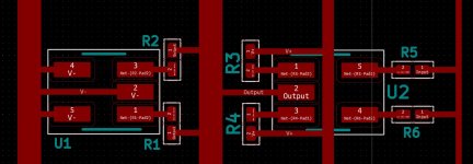
One side of my board is a ground plane and the other side is an output node copper pour.
It would be interesting to know if there is an all-N version among the 4 Nelson is evaluating and if so, what is the topology.
In an all-N version, the bottom half can be one or two MOSFETs to reduce board area.
Hope you made it in (few) blinds leading bunch of blinds fashion
that's at least how I would try it as first
De parabel der blinden

that's at least how I would try it as first
De parabel der blinden

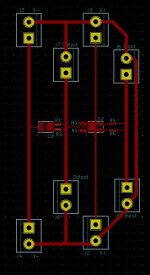
The first PCB design is finishing and should be to me within a week.
Next I want to make a more scalable design that can be as small or large as desired with one or many of a basic one-column many-row layout.
This will be surface mount, assembled at the same place that makes the PCBs.
There are some decisions to make as to circuit topology and devices to use.
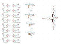
1. Topologies
a. complementary N-P
b. single ended all N
c. Mu follower all N
suggestions for other topologies?
devices
a. J270 this is the only P device that I can find with gain commensurate with Idss
b. 2SK2145
b. 2SK208
c. 2SK209
This is where you vote for topology and devices. I will have some of these made and share as needed. I can open a group buy thread in the group buy forum if it gets to that.
Next I want to make a more scalable design that can be as small or large as desired with one or many of a basic one-column many-row layout.
This will be surface mount, assembled at the same place that makes the PCBs.
There are some decisions to make as to circuit topology and devices to use.
1. Topologies
a. complementary N-P
b. single ended all N
c. Mu follower all N
suggestions for other topologies?
devices
a. J270 this is the only P device that I can find with gain commensurate with Idss
b. 2SK2145
b. 2SK208
c. 2SK209
This is where you vote for topology and devices. I will have some of these made and share as needed. I can open a group buy thread in the group buy forum if it gets to that.
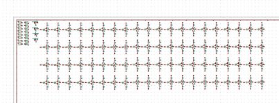
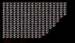
Laid out a B1 buffer with 2SK2145 so that the basic buffer cell can be copied vertically in a column.
With this initial layout, I can possibly get 2,000 buffers on one board 14" x 21". Each 2SK2145 is two JFETs. This assumes using both sides of the PCB. This layout only requires one layer. The idea would be to mirror this layout on the bottom layer. The two layers would share V+, V+, Input, Output terminal blocks.
I think this layout can be reduced by using terminal blocks with 1/2 size spacing. This layout uses 0.2" terminal block spacing.
Attachments
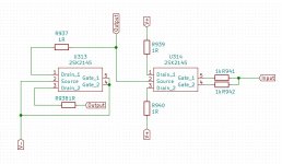
Here is what I think is the "optimal" layout for the buffer. It consumes 0.2 inches^2. It is two of the 2SK2145
This is 4 transistors comprising two parallel buffers.
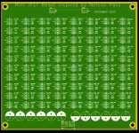
The NP original Beast 14" x 21" board costs double extra because of large size and is larger than needed for the SMT version.
The plan is to make a 10" x 12" board with room at the top and bottom for power and signal terminal strips.
1000 pcs of 2SK2145 should fit on one side. It will be 1000 B1 buffers in parallel.
Using the Y grade of the 2SK2145, it should be possible to run at + / - 15V and not have power dissipation problems at each device.
Bias current will be at least 1.2A, probably closer to 2A.
This is 4 transistors comprising two parallel buffers.
The NP original Beast 14" x 21" board costs double extra because of large size and is larger than needed for the SMT version.
The plan is to make a 10" x 12" board with room at the top and bottom for power and signal terminal strips.
1000 pcs of 2SK2145 should fit on one side. It will be 1000 B1 buffers in parallel.
Using the Y grade of the 2SK2145, it should be possible to run at + / - 15V and not have power dissipation problems at each device.
Bias current will be at least 1.2A, probably closer to 2A.
Attachments

Interesting!
Will these boards be available in DiyStore when finished and tested?
If a jfet fails.....is it possible in some way to find out which?
Don't know if rows can be coupled in and out or there is a smart way to do measurements to find a failing jfet?
If they have gate resistors.....the usual way is to measure "gate current"?
Interesting!
Will these boards be available in DiyStore when finished and tested?
If a jfet fails.....is it possible in some way to find out which?
Don't know if rows can be coupled in and out or there is a smart way to do measurements to find a failing jfet?
If they have gate resistors.....the usual way is to measure "gate current"?
Good questions. I designed it so that every single JFET can be measured and disabled. I used drain resistors similar to the XA25.
Attachments
...and.... I doubt anyone wants to hand solder 1000 of the 2SK2145 and 3000 resistors for a stereo pair. Twice that many for a balanced pair.
I plan to have a stereo pair assembled by the same board house that makes the boards.
I will assemble the through-hole headphone version.
If it works, I will offer a group buy.
I am using this project to learn Kicad.
I plan to have a stereo pair assembled by the same board house that makes the boards.
I will assemble the through-hole headphone version.
If it works, I will offer a group buy.
I am using this project to learn Kicad.
- Home
- Amplifiers
- Pass Labs
- Beast with 1000 JFETs redux?