No heatsink is a big plus for me too. And the amplifier is scalable.
It's a very interesting project.
Yes scalability is a benefit. I can make a small version to learn and make a much larger version when ready. Speaking of that, if there are any Kicad experts who want to participate, we could make open source sub-circuits for people to use as desired. The largest time sink is cloning and arranging the cells. The tools to make these massively parallel row-column arrangements are not native to Kicad. One of the plugins that should help so far has been a disappointment.
The DC filtering and current distribution need attention.
Wouldn't it be better to use a layer for each DC rail, and then short via to where's needed??
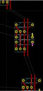
After thinking about it I tried a 4-layer layout and it looks much denser and eliminates two of the buses.
The DC filtering and current distribution need attention.
Wouldn't it be better to use a layer for each DC rail, and then short via to where's needed??
Here is the buffer cell laid out for a 4-layer board. The cell packs much more compact than a 2-layer board.
Attachments

This is a version for TO-92 devices?
Yes. TO92 Drain-Gate-Source pin footprint. 80 parallel complementary buffers.
If your average JFET is 3 mA Idss, total bias current will be ~ 240mA from both power rails.
Your PCB layout went well but I suggest to place some ventilation holes in PCB.
I remember Elektors D.Self parallel NE5532 power amp. The opamps in the middle of the PCB went pretty hot compared to opamps at the edges because of difference in air flow. The copper in a 4-layer will help to distribute heat also, but I guess some ventilation holes would support to keep temperature raise low.
I remember Elektors D.Self parallel NE5532 power amp. The opamps in the middle of the PCB went pretty hot compared to opamps at the edges because of difference in air flow. The copper in a 4-layer will help to distribute heat also, but I guess some ventilation holes would support to keep temperature raise low.
Your PCB layout went well but I suggest to place some ventilation holes in PCB.
I remember Elektors D.Self parallel NE5532 power amp. The opamps in the middle of the PCB went pretty hot compared to opamps at the edges because of difference in air flow. The copper in a 4-layer will help to distribute heat also, but I guess some ventilation holes would support to keep temperature raise low.
Good question. If you look at Nelson's article, the PCB is on its edge and the enclosure is vented.
Even if I mount it horizontally, I would use a well ventilated enclosure.
Toshiba used to make a great laptop. It had hundreds of tiny holes in the laptop enclosure and it needed no fan.
I think Toshiba still makes n-channel jfets in smd.
Zen Mod has shown the way using the 2SK2145. That device is my next pcb in a B1 configuration.
My next pcb will be 500 pcs of the 2SK2145 arranged in a massively parallel B1 configuration. 1000 JFETs total per channel.
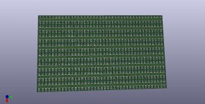
I have been struggling with Kicad to actually lay out 250 identical buffers. Just learned the last step this morning to make that happen.
That is how I spent my two weeks off of the day job.
The TO-92 through-hole flea-powered version is now in production. It may get to me by the end of next week.
In the meantime, the massively parallel B1 starts layout this week.
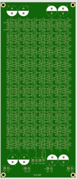
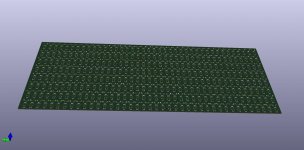
This one is good enough to send for fabrication. It has taken a week to figure out how to get the plugin to place these. Hand route one cell. 639 cells are a clone. All parts have unique sequential part numbers. There are 999 ways to do it wrong and 1 way to do it correctly.
Attachments
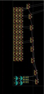
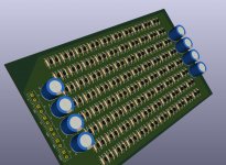
Third iteration of massive complementary buffer. 80 buffer pairs for headphone usage and flea power speakers.
6-layer board allows no hand routing between buffers. I only had to route one buffer and clone the rest. The cloning plugin also can arrange a matrix of identical circuits.
All of the circuit nodes have their own copper layer.
6-layer board allows no hand routing between buffers. I only had to route one buffer and clone the rest. The cloning plugin also can arrange a matrix of identical circuits.
All of the circuit nodes have their own copper layer.
Attachments
- Home
- Amplifiers
- Pass Labs
- Beast with 1000 JFETs redux?