Could you share the link of the amp you referring.Not forget that I still used the 2N3055.
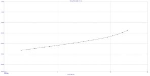
Rows of 7 x BD139 /140 give -140 dB @ 1W
I tried. To bias common emitter with bjt is pain in the ***. I would just go with mosfet. It actually makes more sense for mosfet. The high threshold voltage of the mosfet is not an issue with common Source configuration. Also you get rail to rail output voltage swing.
My bias towards class B. It is just my preference. I could put 1A bias and run 1W, but the software I use only has 0.001% resolutions.


EF + mirror and ccs on the ips : THD @ 1W -131 dB
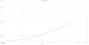
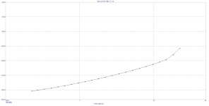
0.0000275 %
this
- is the THD_1k(1W_8Ohm), which I read for my recommended iteration of the A1, i.e. MC12
- also corresponds to your statement after playing Bernhard's last trump card!
In the interesting range, above 1W to 10W, my THD plots are much flatter than yours. Unfortunately, you lost this match by a very narrow margin, and you should accept that.
It might be interesting for the reader to clarify why our two 1W-THD-Things don't differ, and can't differ much at all - where MC12 gets this insane resolution from is also interesting.
Can MC12 (for example) predict the crazy value of -240dB?
HBt.audio
PS
The explanation is quite simple, but I won't reveal the secret, it's trivial and known to every professional designer.
Can MC12 (for example) predict the crazy value of -240dB?
Do you mean... like this ?
Attachments
ref post#187
This is exactly the design I'm talking about. Have you finally been able to patent it in the last five years? As soon as you succeed in implementing it in reality (the real world, outside of the MC12 simulator), you'll be a man made and really shake up the high-end circus.
I wish (and wish) you every success.
HBt.
Psst
The rest of us assume that at some point you will present this ultimate power amplifier to the public.
Perhaps the picture in the appendix will help the newcomer to understand - and differentiate.
(?)
#
Let's end the THD war now, because we will never be able to confirm these dream values in reality, in an actual power amplifier. That should be quite clear to any (professional) designer.
An A1 is no longer an A1 if we give him a completely different skeleton. That is the crux of the matter.
(?)
#
Let's end the THD war now, because we will never be able to confirm these dream values in reality, in an actual power amplifier. That should be quite clear to any (professional) designer.
An A1 is no longer an A1 if we give him a completely different skeleton. That is the crux of the matter.
Attachments
The strength is that it is a class A amplifier. It has zero crossover distortion.
The weakness is that the gain and output current drive are both low. As a result of low gain, distortion is high. The output has significant hum as Stereophile measured.
One can actually hear a very quiet 100Hz tone directly at the speaker membrane.
The only thing missing for our crystallizing A1 reboot forum project is a correctly dimensioned power supply unit.
Any suggestions?

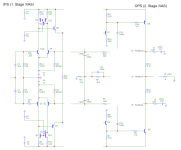
Another quick "No".It is redrawn by me, is it the same as yours functionally and correct?
It is not my schem, it is not correct!
I realize that,
so I'm attaching the circuit again - you can check it yourself. The models are known or can be found in the “Stellema thread”.
You might also like to try out the extension from posting #153.
Good luck with it.
#
I'll wait and put my money on “M0rton”.
Your schematic from this post, I redraw it, only want to know if I made any errors.
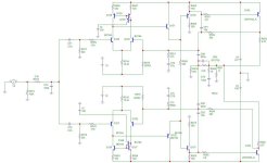
These are the two topologies that face each other here.
Both have 4 junctions in the signal path from input to output.
A1: ips - ef - ef - vas
My modification: ips - vas - ef - ef
Just a different arrangement.
Both have 4 junctions in the signal path from input to output.
A1: ips - ef - ef - vas
My modification: ips - vas - ef - ef
Just a different arrangement.
A very decisive difference,
it is by no means as marginal as you would like to portray it here.
Either you can't distinguish the fundamental connections or you simply don't want to. Perhaps it's a question of education, a misunderstanding or simply a lack of specialist knowledge and the competence to make a fundamental analysis?
I'm completely at my wit's end. I am sorry.
Unfortunately, your line-by-line description of the two fundamentally different concepts is misleading and simply not really 100% correct.
This whole number is slowly becoming a farce.
Dear Bernhard,Voltage controlled current sources with feedback, to be precise.
As much as I would like to "like" this statement - it is also incorrect. The MF-A1 voltage amplifier is not a voltage-controlled current source.
I suspect that I can guess in the broadest sense what you are referring to - and because you are honored by this, I have “liked” your post.
#
Principle, i.e. debates about being right
do not belong in this thread and do not help anyone here.
Let's not just play down the fact to "the small difference." That's the only thing I want, because the difference is enormous.
I'm very tired now, these unnecessary arguments are exhausting me.
Bye,
HBt.
PS
"Just a different arrangement" [Bernhard]
👍
And that number is now also off the table. Blameless goes A1 - just equal, but different!
🙄
- Home
- Amplifiers
- Solid State
- An A1 descendant - a relentless analysis