When correctly biased with 12 volts at the midpoint both transistors should be equally hot.
If the fault causing your 20 volt midpoint is due to the input FET not conducting then both will be cold because no current can flow in either due to Q1 (the lower FET) being off.
If you add the resistor across the FET you turn Q1 fully on. That means little voltage is across it but it still sees the full output stage current of around 1.6 amps. Q1 runs cold. Q2 however sees around 22 volts across as well as the current. Q2 gets hot (power is volts multiplied by amps).
So the input FET not conducting and adding the resistor as a test give two different scenarios. Both will give 20 volts midpoint but one (non conducting FET) has no output stage current flowing and the other (adding the resistor) should see the full 1.6 A

So far I was able to do these tests
“What is the voltage on R6? (it doesn't matter which end you measure to)”
Right board 3.4V
Left board 3.6V
“What is the voltage on R10? This is the gate of the input FET.”
3.2V Right board
3.4V Left board
“Other possibilities are a problem with the connection from Q1 gate via R6 to the input FET. Confirm you measure 100 ohms from the gate pin of Q1 itself (measure from the pin and not the board) to the input FET source pin. You can check that in circuit. It should read approx 100 ohms.”
Q1 gate to Q4 source
Left board 103ohm
Right board 99.4 ohm
I’ve ordered the other resistors to test Q1 and 2. Thank you for the explanation regarding Q1 and 2.
Last edited:
This is a puzzling one. I suspect something around the input FET (or the FET).
3.6 volts on R6 isn't quite enough to get the power FET into conduction.
Look at R10 (330k) that connect the gate of the input FET to the preset wiper.
You should see approx the same voltage on either end of the 330k. Check that is so first. The actual voltage depends on the preset position and should be able to be taken down to zero volts at one end of the range and as high as whatever the midpoint voltage is at the other end.
A totally random thought. If the input cap C3 is fitted incorrectly (wrong way round) then the leakage current would be enough to pull the gate voltage down. That scenario will show by you measuring very different voltages on each end of the 330k
Attachments
-
 8065BF1B-231D-4939-BA1B-BCE6C4B69928.jpeg413.9 KB · Views: 112
 -
 B6F9DC16-A435-47C2-B19A-F315ACAB2C04.jpeg386.5 KB · Views: 122
 -
 39C6DBDB-BD6C-48CD-93CA-CC669DD72552.jpeg429.2 KB · Views: 115
 -
 9E33D0C2-8504-4768-91E7-E598DF4BE341.jpeg319.1 KB · Views: 114
 -
 AFAA174A-5080-4E40-ACD6-D1B803452BBB.jpeg448.6 KB · Views: 113
 -
 EC52CA8F-5C7C-4C0C-8C17-6FA30F86C4F8.jpeg433.4 KB · Views: 112
 -
 57E8E9CC-6899-4CFF-B81A-C4D3AACF1309.jpeg465.9 KB · Views: 114
 -
 25D485AC-CA2F-4CF9-8FA3-0527F2E766E2.jpeg377.3 KB · Views: 107
 -
 73B3F598-21CB-4803-9A0E-9BB6E0A24C26.jpeg363 KB · Views: 112
 -
 934D36E2-1F02-4817-B58C-B6F56B706842.jpeg433.8 KB · Views: 108
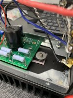
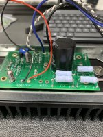
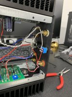
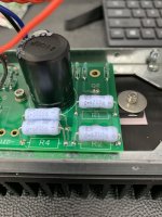
I’ll share the results of the test, wanted to share some pictures first, I tested all the resistors before I populated the board, individually. They were the correct values. Capacitors are all facing the correct way for polarity. I pulled the boards to make sure nothing was touching the chassis and that’s good also. Testing now.
“You should see approx the same voltage on either end of the 330k. Check that is so first.”
I get 3.4Volts on either end of R10.
“The actual voltage depends on the preset position and should be able to be taken down to zero volts at one end of the range and as high as whatever the midpoint voltage is at the other end.”
Do I do that by adjusting the potentiometer?
I get 3.4Volts on either end of R10.
“The actual voltage depends on the preset position and should be able to be taken down to zero volts at one end of the range and as high as whatever the midpoint voltage is at the other end.”
Do I do that by adjusting the potentiometer?
I’m just going to de solder everything and individually test the components as I go. I’ll chalk it up to a learning experience.
I'm not sure (well I am sure actually 🙂) that that is a good idea. Ideally any fault should be found by doing as minimally invasive work and testing as possible.
As for the input FET, well I think the circuit should bias up OK if that were even swapped to a small signal NPN transistor like a BC546 or similar.
As for the input FET, well I think the circuit should bias up OK if that were even swapped to a small signal NPN transistor like a BC546 or similar.
Q3

Q4

Q1

Q2

C1=2851uf
C2=966uf
C3=10uf
C4=11uf
R1=.5 ohm
R2=.5 ohm
R3=.7 ohm
R4=.7 ohm
R5=100 ohm
R6=99.5 ohm
R7=10k ohm
R8=1k ohm
R9=1k ohm
R10=331k ohm
R11=10k ohm
R12=39k ohm
R13=32.96 ohm
R14=1k ohm
R15=2.2k ohm
These are the values for the left channel as I pulled each one out. I still have the right channel to do.
I ought to have left the components in, and gone from there. However I really wanted to see if I had put something in a incorrect spot.
I ordered a new parts kit for it anyway.
Q4
Q1
Q2
C1=2851uf
C2=966uf
C3=10uf
C4=11uf
R1=.5 ohm
R2=.5 ohm
R3=.7 ohm
R4=.7 ohm
R5=100 ohm
R6=99.5 ohm
R7=10k ohm
R8=1k ohm
R9=1k ohm
R10=331k ohm
R11=10k ohm
R12=39k ohm
R13=32.96 ohm
R14=1k ohm
R15=2.2k ohm
These are the values for the left channel as I pulled each one out. I still have the right channel to do.
I ought to have left the components in, and gone from there. However I really wanted to see if I had put something in a incorrect spot.
I ordered a new parts kit for it anyway.
Attachments
I don't think you will find a problem this way tbh.
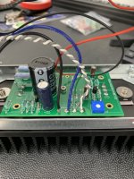
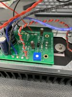
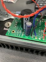
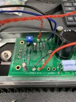
If you place R15 (the 2.2k) across the Drain and Source of the input FET (Q4) does the midpoint voltage drop right down? That would show the output stage is basically working.
Like this.

If you place R15 (the 2.2k) across the Drain and Source of the input FET (Q4) does the midpoint voltage drop right down? That would show the output stage is basically working.
Like this.
Mooly, I wanted to say thank you for all your assistance. I ordered in a new parts kit, and kept the chassis. I soldered everything up, I did use silver tinned wire this time though and 12Ga wire for power. I was talking with Gareth Roberts and he corrected something I did wrong on the first build, which was most likely the issue, I thought I was supposed to set the dc offset to 20V. This time I set it to 12V (actually 12.04 and 12.06, I couldn’t get them any closer.) It works fantastic!


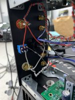
Hey all, I've come to step 39 ( Back Panel Wiring 3 ) and realized I'm missing the green wire that is mentioned. I'm sure I can find some at the local hardware store or amazon however I don't know what gauge of wire it's supposed to be. I have lots of 12, 14 and some 18 and I figured it probably wouldn't hurt to upsize the wire but I wasn't sure how sensitive the components are to voltage differences caused by the resistance of the wire.
LED- is 22awg black in the V1.8 kit.
In- is 22awg grey in the V1.8 kit.
https://cdn.shopify.com/s/files/1/1006/5046/files/ACA_wiring_-_All_Together_-_V18.pdf?v=1593415056
I hope that assists.
In- is 22awg grey in the V1.8 kit.
https://cdn.shopify.com/s/files/1/1006/5046/files/ACA_wiring_-_All_Together_-_V18.pdf?v=1593415056
I hope that assists.
Hey all,
I got the 1.6 version of the amp that I first assembled in a wooden case in 2020. So far it got super nice but since I didn't have time to finish properly the enclosure I decided to get the aluminium one a few days ago.
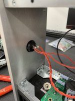
So I decided to transfer the whole set up into the aluminium case, and realizing that the DC power input jack wires were too short compared to my wooden setup to reach the rear panel, I just soldered it the wires witout attaching the barrel connector to the panel, you know, just for the test. And then it got wrong... While the amp being turned on, I observed a little crack on the little tab of the barrel connector. What I suppose is that the red twisted pair of wires touched the ground bus.
And now, only one PCB delivers the sound. I guess the other one burnt somewhere but I dunno where to start checking ? Could you guys please orientate me in the diagnosis ?
Thanks in advance, best regards. Baptiste.
Ps: sorry for my english, I'm doing my best though.
I got the 1.6 version of the amp that I first assembled in a wooden case in 2020. So far it got super nice but since I didn't have time to finish properly the enclosure I decided to get the aluminium one a few days ago.
So I decided to transfer the whole set up into the aluminium case, and realizing that the DC power input jack wires were too short compared to my wooden setup to reach the rear panel, I just soldered it the wires witout attaching the barrel connector to the panel, you know, just for the test. And then it got wrong... While the amp being turned on, I observed a little crack on the little tab of the barrel connector. What I suppose is that the red twisted pair of wires touched the ground bus.
And now, only one PCB delivers the sound. I guess the other one burnt somewhere but I dunno where to start checking ? Could you guys please orientate me in the diagnosis ?
Thanks in advance, best regards. Baptiste.
Ps: sorry for my english, I'm doing my best though.
@batiste
Refer to step 56 of the guide and please measure and record voltages on your inoperative PCB.
https://guides.diyaudio.com/Guide/Amp+Camp+Amp+V1.6+Build+Guide/5?lang=en
Refer to step 56 of the guide and please measure and record voltages on your inoperative PCB.
https://guides.diyaudio.com/Guide/Amp+Camp+Amp+V1.6+Build+Guide/5?lang=en
2 1/2 years ago built the v1.16 stock kit to use as a stereo amp. Best I can judge it works fine.
Last week completed building the v1.18 stock kit. Again, best I can tell it works fine.
The v1.18 runs a little cooler than the v1.16
The v1.18 does not make that sound heard through the speakers when its first turned on.
Built the second ACA to use them in balanced or parallel mono.
In balanced mono the music played only half as loud.
I have very efficient speakers; 8 ohms 95db.
Was informed that in balanced mono the amp now sees the speaker as an 4 ohm load, which may account for the lesser volume output.
The v1.16 only has a two position switch. For parallel mono I assume that the v1.16 switch should be up in the mono position. Yes?
Or must I buy the parts to update the v1.16 so it matches the v1.18 back panel wiring and component configuration?
Thank you for consideration of my question.
Best.
Michael
- Home
- The diyAudio Store
- Amp Camp Amp Kit 1.6/1.8