Hi X,
first link is only a list 23 results 0,22 Ohm/3W resistors.
If you scroll you also find ERX-3SJ or KOA MOSX typ.
My experience is not as good as yours, so thanks for the tip, i will not use
wirewound for degeneration R. 🙂
Could also good work MPC 71 in that position?
MPC71 0R1 K | Fukushima Futaba Serie MPC Metallplattenwiderstand, 100mΩ +-10% 5W | RS Components
Those look just like the KOA Speer BPR series - metal alloy Ni/Cr/Fe/Cu mix to achieve correct resistance. I am not sure if they are not as good as Pan ERX yet without definitive tests - but I fear that heating Fe containing metal wire produces some strange behaviors. Kind of like why cheap Aliexpress steel leads metal thin film is not as good as Yageo copper lead metal thin film resistors from distortion standpoint. I have measured this and seen a minor difference on circuits. The Dale CMF are also copper leads so work well too.
Hi Bangla,
Closer to home you have the excellent Manganin PBH resistors from
Isabellenhütte at Buerklin or Distrelec
They're the one of the best in the Resistor Current Noise Measurements
Regards,
Danny
Closer to home you have the excellent Manganin PBH resistors from
Isabellenhütte at Buerklin or Distrelec
They're the one of the best in the Resistor Current Noise Measurements
Regards,
Danny
Very wise decision voltwide....let the guys do their business here 🙄
are you going to disable your account too daanve? that would be very wise
Hi X,
I was looking at getting ahead of the game and have copied all yours and Hugh's interesting and helpful advice along the way in this thread.
Up to now and what appears to having been successfully tested with your prototype boards, have you made any changes to the schematic you have been working to?
I have looked at post #1 where you have been updating along the way looking for the final schematic and a BOM that lines up with your build.
Is it possible to post these if you might have them ready to publish?
I would like to see what I might have that I can use and then start preparing a Mouser project for what I need to buy, ready for when you might have the pcb's available to send out in the New year.
Best Regards,
Gary..
Hi Gary,
Vunce is building his right now and had some good questions for me as to which components to use because the schematics have dual values at certain points for the compensation caps, and even one of BJT’s (Q4 on Hugh’s diagram). I am checking with Hugh on compensation cap values as there was one that was specified as either 5pF, 7pF, or 10pF. I think that one might just be down to trial and test via O-scope and listening. I currently have 22pF there. Another spot is which way to orient the diodes on the snubber boards. There is a little bit of collecting the comments and notes but the short story is, the BOM as is, works great. I think Vunce might have some comments.
C122/1220 I am using 4700pF or 4.7nF film cap.
R113 I am using 22R, but there is a socket there for a trimpot. Offset is +2mV per 100R. I am getting -3mV so maybe optimal value is about 150R to 200R.
V131 should be KSA992 even though it says BD140 on schematic. Actually BD140 would work too - just make sure pinouts correct.
As for the source resistors, the BPR’s work and I am exploring if using Panasonic ERX series there or fancy TO-247 (Isabellenhutte PBH-R220-F1-1.0) there works better as far as lower distortion is concerned.
For outputs I am using the larger heat rated Fairchild FQP’s with ceramic spacer pads and thermal compound.
For snubber boards, use small piece of Kapton tape over the components to make sure legs of MOSFET doesn’t short out.
Regarding boards, I have the new Gerbers (just a few tiny changes to make more room for the minifit connector levers, and add optional Faston tabs for speaker outputs) and now need to start a GB thread to start taking pre-orders. Will order in about 1 week and boards should be back another 10 days. You might get it by x-mas or New Year?
Last edited:
Caddock thick film? This might not be any good as I recall thick film SMT on feedback resistors produced higher H3. But here is an interesting choice as TO-126. Would require a small stamped aluminum flag heatsink. They didn’t have 0.22R. The 0.15 ohm would be for someone looking to boost bias current to over 2A possibly for lower impedance load. Thermal dissipation of amp would go up to about 120w per channel.
MP915-0.15-1% Caddock | Mouser
MP915-0.15-1% Caddock | Mouser
Last edited:
Thanks for the reply in post #310 X, so I take it from reading your response there that a revised schematic and BOM to suit will be coming in the near future to this thread. No hurry as this will be a project for mid next year for me.
Cheers,
Gary..
Cheers,
Gary..
Yes, I will get a final version of the schematic and BOM out once I have some time and get all the comments back from Vunce and Hugh.
The GB Thread has been created:
https://www.diyaudio.com/forums/gro...na-39w-se-class-amplifier-gb.html#post5993558
Technical discussions in this thread. Please refer all ordering or GB questions in the other thread.
The GB Thread has been created:
https://www.diyaudio.com/forums/gro...na-39w-se-class-amplifier-gb.html#post5993558
Technical discussions in this thread. Please refer all ordering or GB questions in the other thread.
Last edited:
The GB Thread has been created:
Hi X,
Does the same pcb apply to the lower power 20W, lower heat build?
Cheers,
Jacques
YES Jacques no change except resistors on the LTP stage current must be set to pass 2.6mA.
You can adjust the stage current to bring offset down to 0mV.
HD
You can adjust the stage current to bring offset down to 0mV.
HD
Last edited:
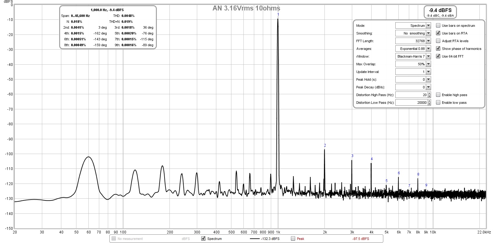
The fact that the board is completely connectorized (9 total) allowed me to pull it out of the chassis in 2 minutes, swap the KOA 0.22R J BPR soure resistors for Panasonic ERX 0.22R 3W, and reinstall in 2 minutes, and then take another measurment at 3.16Vrms (1W) and 10ohms to compare, is very handy. It sure is nice to have remotely mounted MOSFETs!
I am very surprised that the venerable Panasonic ERX has now been declared no longer the King! The KOA BPR is superior! KOA BPR measured 0.0048%THD and Panasonic ERX measures 0.0054% THD. Profile is a tiny bit higher in even orders, especially 4th order with the ERX I think, but not enought to justify the increase in THD. I guess we will be spec'ing KOA BPR's from here on out. They are more readily availble, take up less real estate, and are rated 5W vs 3W which is a great bonus.
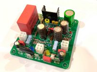
Here is the board with the ERX's installed:

Here is the FFT from the KOA BPR's for reference:
Here is the FFT from the Panasonic ERX:

I guess this lays this question to rest - the one's specified in the BOM are good to go.
What is interesting is that at higher power of 12W, the THD and FFT profile is about the same. So it seems to affect the 1st watt more.
Here is 12W witj KOA BPR for reference:
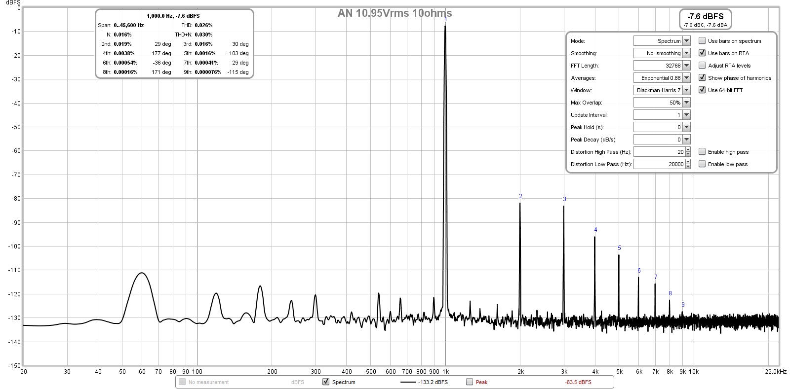
Here is with the Panasonic ERX:

I am very surprised that the venerable Panasonic ERX has now been declared no longer the King! The KOA BPR is superior! KOA BPR measured 0.0048%THD and Panasonic ERX measures 0.0054% THD. Profile is a tiny bit higher in even orders, especially 4th order with the ERX I think, but not enought to justify the increase in THD. I guess we will be spec'ing KOA BPR's from here on out. They are more readily availble, take up less real estate, and are rated 5W vs 3W which is a great bonus.
Here is the board with the ERX's installed:
Here is the FFT from the KOA BPR's for reference:
Here is the FFT from the Panasonic ERX:
I guess this lays this question to rest - the one's specified in the BOM are good to go.
What is interesting is that at higher power of 12W, the THD and FFT profile is about the same. So it seems to affect the 1st watt more.
Here is 12W witj KOA BPR for reference:
Here is with the Panasonic ERX:
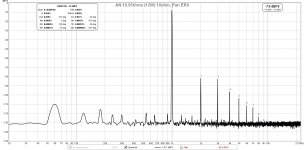
Attachments

Last edited:
Hey
The plastic case on modern flat transistor packages gets darn hot and it never makes sense to me that people clamp this face hard against a PCB. For best heat management, the plastic face should be exposed to air. One can easily burn up a PCB otherwise.
For me SM parts are a no-go - vision not good enough. besides, it is sufficient to place the gate protection zener right at the mosfet pins, as should be its gate-stop, and these can be through-hole parts. never had an issue doing it this way for a couple of decades so far...
Looking at your build photos in post-1, it seems to me that the grounding and wire twisting is not done correctly, otherwise the 50Hz in the output noise spectrum would be absent. I have not looked at the whole thread; is there a schematic of your power supply? There should be local filtering on each PA card.
The signal ground should not star with the AC ground; rather, the AC ground being noisy and for protection should be on its own lug. The signal ground should tie to chassis on its own lugs through a ground-link-isolator circuit (anti-parallel diodes in parallel with C and parallel with R).
Othewrwise, your boards, chassis and work space look really nice 🙂
Hi Nauta,
The SMT on the main board are optional as there are through hole alternate pads on other side. Except the output Thiele network, that is an SMT but an easy one. As far as the snubber boards go, the ideal spot is next to legs. You are welcome to deadbug a TH part there.
As far as grounding goes, here is the diagram as built:
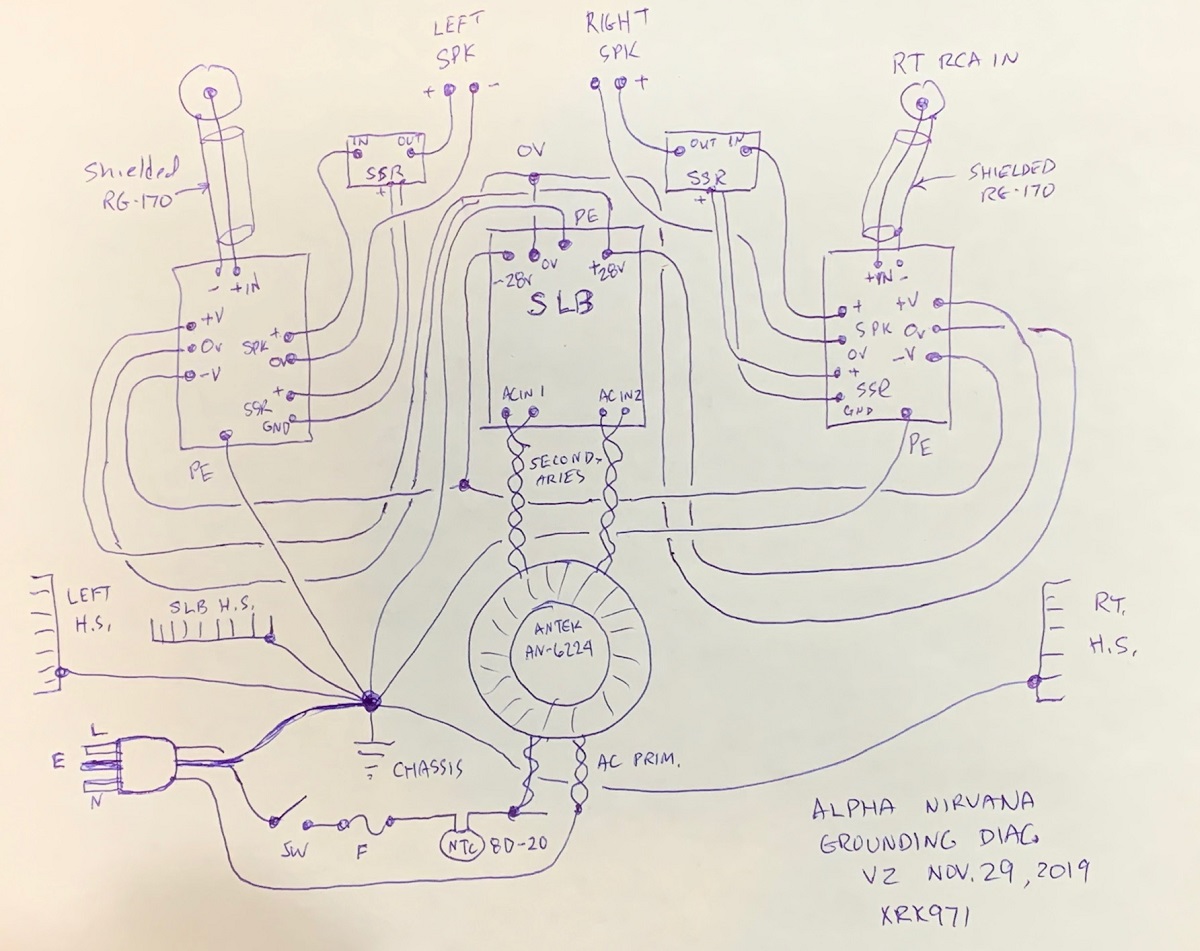
Each board has its own ground loop breaker (GLB) consisting of a CL60 NTC (or 8D-20) and 22nF film cap to earth/chassis GND. The analog signal input ground is not Star topology but each is lifted by 10R relative to power 0v GND which is Star hub topology. The hub is at the SLB PSU, also has its own GLB to earth/chassis. (but on an M2X, it has been shown that star hub on analog audio input makes the hum go away - but that amp has different grounding scheme and no GLBs or ground lift).
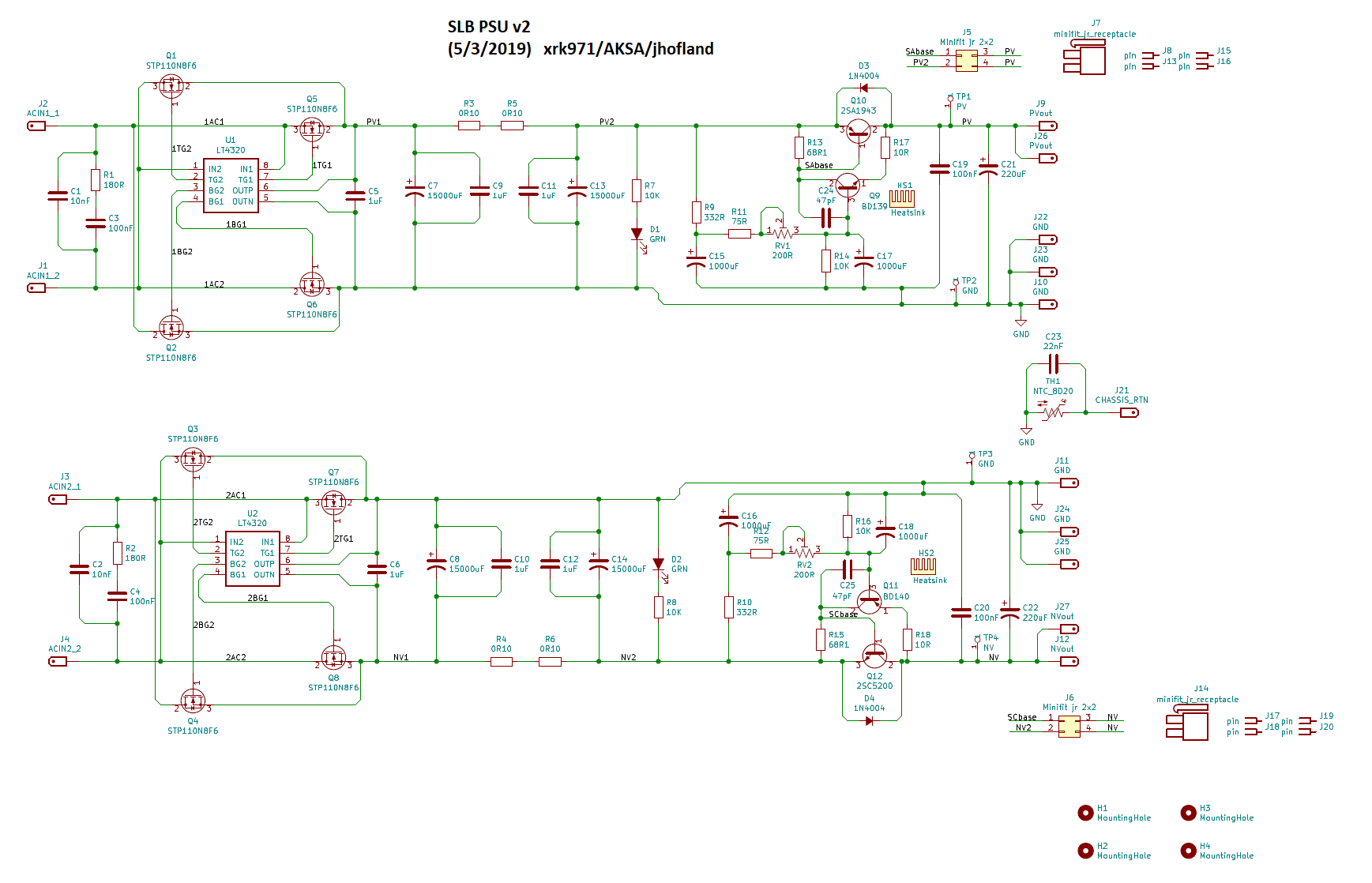
Here is the schematic for the SLB PSU:
Here is Alpha Nirvana schematic in case you want to look at the ground lift and GLB:
https://www.diyaudio.com/forums/att...-class-amplifier-gb-alpha-nirvana_sch_001-pdf
If you can do better than -110dB on the mains 50/60Hz peak on a Class A amp drawing 3.4A - I would like to see your setup and FFT. I have achieved absolute noise free baselines before but generally on SMPS or DC-DC step up PSU - not linear toroidal trafo mounted in same cabinet. Just the EMI emitted from that trafo will fly through the air and be picked up by the amp. No amount of ground loop prevention stops that. Only mu-metal or steel shielding boxes or a separate chassis for the PSU.
As for heat from MOSFETs - the snubber boards are 2mm thick FRP covered with 2oz copper and via stitched to form an excellent thermal conductor. If PCBs can take soldering or hot air ovens at 150C without fear, the 70C temps on the PCBs from the MOSFETs are not going to be an issue. They work very well to actually increase surface area of the epoxy case and serve as a small radiator. When we use these with a clamp bar on a CPU cooler, their job is to conduct heat through and via stitched copper pours are well known to be effective heatsinks.
The SMT on the main board are optional as there are through hole alternate pads on other side. Except the output Thiele network, that is an SMT but an easy one. As far as the snubber boards go, the ideal spot is next to legs. You are welcome to deadbug a TH part there.
As far as grounding goes, here is the diagram as built:
Each board has its own ground loop breaker (GLB) consisting of a CL60 NTC (or 8D-20) and 22nF film cap to earth/chassis GND. The analog signal input ground is not Star topology but each is lifted by 10R relative to power 0v GND which is Star hub topology. The hub is at the SLB PSU, also has its own GLB to earth/chassis. (but on an M2X, it has been shown that star hub on analog audio input makes the hum go away - but that amp has different grounding scheme and no GLBs or ground lift).
Here is the schematic for the SLB PSU:
Here is Alpha Nirvana schematic in case you want to look at the ground lift and GLB:
https://www.diyaudio.com/forums/att...-class-amplifier-gb-alpha-nirvana_sch_001-pdf
If you can do better than -110dB on the mains 50/60Hz peak on a Class A amp drawing 3.4A - I would like to see your setup and FFT. I have achieved absolute noise free baselines before but generally on SMPS or DC-DC step up PSU - not linear toroidal trafo mounted in same cabinet. Just the EMI emitted from that trafo will fly through the air and be picked up by the amp. No amount of ground loop prevention stops that. Only mu-metal or steel shielding boxes or a separate chassis for the PSU.
As for heat from MOSFETs - the snubber boards are 2mm thick FRP covered with 2oz copper and via stitched to form an excellent thermal conductor. If PCBs can take soldering or hot air ovens at 150C without fear, the 70C temps on the PCBs from the MOSFETs are not going to be an issue. They work very well to actually increase surface area of the epoxy case and serve as a small radiator. When we use these with a clamp bar on a CPU cooler, their job is to conduct heat through and via stitched copper pours are well known to be effective heatsinks.
Last edited:
Alpha Nirvana 39W SE Class A Amplifier GB
by Hug Dean (AKSA)
Military up to 90 dB.
Then, how much decibels attenuates the avionics standard? And the Alpha Nirvana PCB 😉
by Hug Dean (AKSA)
Commercial PCB shields from RFI up to 60 dB.JPS's pcb layout is avionics standard, his pcbs are a work of art and his skills are the result of thirty years in the industry. If you build this amp you will be combining SOTA design (it's taken my 30 years to get to this point too!) with professional aerospace layout techniques...
Military up to 90 dB.
Then, how much decibels attenuates the avionics standard? And the Alpha Nirvana PCB 😉
Last edited:
Just a comment - the earth from the mains should really go to a separate lug to meet safety standards.
Hi Maty,
With all the plating around the pcb for strength and thermal management, it should be high. BUT it would have to be measured with some very expensive gear I don't have, nor does X I think. It's an RFI field meter as I understand........
HD
With all the plating around the pcb for strength and thermal management, it should be high. BUT it would have to be measured with some very expensive gear I don't have, nor does X I think. It's an RFI field meter as I understand........
HD
Just a comment - the earth from the mains should really go to a separate lug to meet safety standards.
There is a whole terminal block with nothing but earth ground connections. See large double twisted green wire from IEC to block next to trafo? That then fans out to chassis and the PE connection on each board. Each board has 7A NTC connecting it’s 0v GND to mains earth/chassis.
I think JPS64’s layout using the stitched vias is more for decreasing electrical impedance for the large current carrying paths than anything. The RFI shielding is probably no more than the usual ground plane where possible. Mostly it is the RFI filter on the input (220pF and 2k2) and the Thiele network on the output 100nF series 10R will block ingress of RFI from front and back ends.
Last edited:
- Home
- Amplifiers
- Solid State
- Alpha Nirvana 39w 8ohm Class A Amp