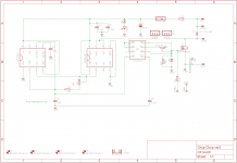
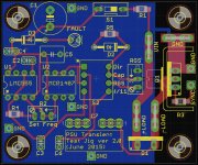
Schematic in post#580 does not match layout. S1, R4, R5 and possibly more, missing from schematic. Congratulations on performing a bit of circuit design mathematical juggling; you will find it a recurring necessity.
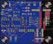
I see three nets routed on the blue layer which could be moved to the red layer, healing the axe-wounds to the blue ground plane. The easiest appears to be LMC555 pin 6 to pin 2; the other two might be slightly more difficult.
I see three nets routed on the blue layer which could be moved to the red layer, healing the axe-wounds to the blue ground plane. The easiest appears to be LMC555 pin 6 to pin 2; the other two might be slightly more difficult.
Oops. Correct one attached.
I will take a look at the routing although I'm not sure even the first one you mention is easy to avoid although I could use vias to shorten up the bottom layer sections. Thanks.
EDIT: got rid of some
I will take a look at the routing although I'm not sure even the first one you mention is easy to avoid although I could use vias to shorten up the bottom layer sections. Thanks.
EDIT: got rid of some
Attachments
Last edited:
Good! What are the pros and cons of rerouting the pin for the oscilloscope ground clip, to have a more direct connection to the GND blade connector? Is it an obviously bad idea? Obviously good? Or some of each?
Given Elvee's previous comments I understood it to be a good idea to try to isolate the ground pin from the transients. It was this that lead me to section the GND plane the way I did.
The ground connection of the chop-box is subjected to the current transients, and the resulting voltage is applied between the grounds of your two probes. They probably drop each a more or less equivalent voltage, and most of this voltage appears on the inputs, because of the finite coupling between the sleeve and the inner conductor and the non-zero screen cutoff frequency.
In such instances, you should ground one channel only, the most sensitive one, and leave the ground of the trigger channel unconnected.
When you absolutely need two sensitive channels with two different reference potentials, there are remediation means, but here you don't need them: just eliminate the ground loop.
I have been trying to do some more digging into this. Section 9 of AN-1733 "Load Transient Testing Simplified" notes that the connection connecting the negative terminal of the transient test jig and the negative terminal of the regulator under test is "most critical" and should be "low inductance or ringing will occur, distorting the current waveform". However, there they seek to observe closely the current waveform from the test jig while here we are merely using the second scope channel as a trigger. Plus, I would have thought any subtlety in the placement of the ground pin would be swamped by the wiring inductance between test jig and PSU under test which I won't be able to minimise to sub-inch runs. That said, a more direct connection to the fasten blade is, it would seem, more technically optimal as it will minimise impedance. If I am to move them, I could place both the Sync pin and the GND pin to the right of Q1.
Last edited:
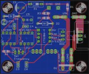
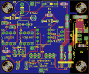
Do what many professional circuit designers do. Put in several ground-clip-attachment-points all over the board, and name them Andy, Beth, Chris, Denise, Edwin, Frieda, Geoffrey, etc. Now you have the option to attach your ground clip at several places and find the one that you like best! Or -- drum roll please -- the ones (plural) you like best. Better to squander fifteen cents on "excess" pin headers, than to wait for another spin of the PCBoard. Some professionals call this "late binding" decision making and/or hedging your bets. Other professionals call it lazy cowardice which indicates fear of decisionmaking.
For example in the attachment, A is the chop chop load resistor's ground and is my personal favorite. B and E* are attempts to get very close to the MCP1407 gate driver IC's ground. Remember that when it discharges the MOSFETs gate, the pulldown current can be several amps. C is the bypass capacitor C1's ground. When MCP1407 pulls the MOSFET gate up, several amperes flow through C1. D and F are attempts to find places on the ground plane that are maximally far away from high current stream-line pathways. In case you ever want to study that.
* Maybe you could scoot C7 south by 150 mils, allowing E to plop right next to MCP1407 pin 4.
Attachments

nice. I think it might still be useful to put text on the schematics and on the PCB silkscreen, naming the various possibilities. Then you can make notes in your lab notebook "I probed the MOSFET gate with respect to groundpoint Alice" or "I connected scope ground to Charlie and viewed the waveform at "ground" point Delta - Wow!" etc. It will also give diyAudio member peufeu an easy way to make unambiguous suggestions about which groundpoints to use for which measurements.
I see a SMALL LOOP AREA for the big currents flowing through the POWER end of the PCB.
That to me means thought has been applied.
That to me means thought has been applied.
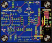
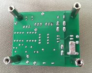
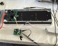
Just finished soldering it up. A little cramped but okay. Tested with 9V battery and no load. Seems to work. Real test still to come with a load. Did not test the Miller cap C7 as need to think about a suitable value from my existing inventory.
Pics: completed board top, bottom showing the braid 'buss bar', gate waveform when no gate stopper resistor, impact of gate stopper (Rgs), impact of Freq/11 switch.
I realised I wasted one of the Switch 2 slots - I could have had the default wiring so that Rgs was engaged and merely used one slot to bypass it (Dir) rather than having switches for Direct and Rgs. Oh well.
More to follow once I get the chance to couple up my PSU and load resistors.
Thanks for all the help!
Attachments

Glad you bought D1 in the ISO-220 package. With no metal slug on the back, it cannot possibly short to the +LOAD and -LOAD spade connectors.
Yes, I was cognisant of that when doing the BoM and board.
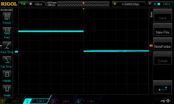
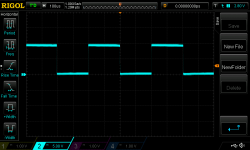
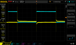
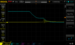
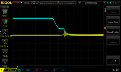
Okay, some initial load transient tests with the new board... They would appear to be a significant improvement on the previous tests.
All these tests were triggered with the trigger channel probe alligator GND clip attached at point "GND A" (see pic 1). There was no pre-load and an 8 Ohm load being switched (c1.5A).
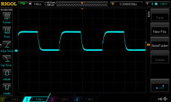
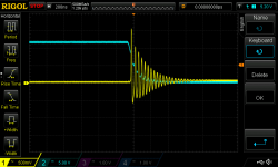
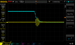
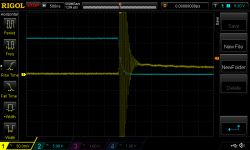
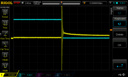
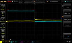
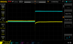
Pics 2-5 are all of the leading edge with increasing zoom on the horizontal axis: 50us, 20us, 2us and 100ns. The chop chop box was set for a hard edge rise/fall (i.e. a direct path to the pass transistor gate, no 'Miller cap' C7). The next 3 look at the trailing edge: 20us, 2us and 500ns.
I was a little concerned by the greater ringing and so I also looked at the trailing waveform when the channel 1 probe was simply in the air versus placed the output of the regulator - pics 9 and 10 (look at the file names for better guidance). I presume there is still some 'interference' relating to inductive ringing on the GND plane but would love to get others' perspectives on this.
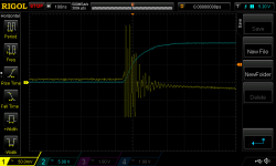
Switching the chop chop box to engage the gatestopper resistor Rgs would seem to confirm this. The last 3 pics are with Rgs resistance at zero and then dialled in first with horizontal divisions of 1us and then 500ns. EDIT: see next post for pics. I find the shape of the chop chop box pass transistor gate waveform, with its pronounced kink, intriguing.
Any and all comments, thoughts, perspectives, suggestions welcome!!
Okay, some initial load transient tests with the new board... They would appear to be a significant improvement on the previous tests.
All these tests were triggered with the trigger channel probe alligator GND clip attached at point "GND A" (see pic 1). There was no pre-load and an 8 Ohm load being switched (c1.5A).
Pics 2-5 are all of the leading edge with increasing zoom on the horizontal axis: 50us, 20us, 2us and 100ns. The chop chop box was set for a hard edge rise/fall (i.e. a direct path to the pass transistor gate, no 'Miller cap' C7). The next 3 look at the trailing edge: 20us, 2us and 500ns.
I was a little concerned by the greater ringing and so I also looked at the trailing waveform when the channel 1 probe was simply in the air versus placed the output of the regulator - pics 9 and 10 (look at the file names for better guidance). I presume there is still some 'interference' relating to inductive ringing on the GND plane but would love to get others' perspectives on this.
Switching the chop chop box to engage the gatestopper resistor Rgs would seem to confirm this. The last 3 pics are with Rgs resistance at zero and then dialled in first with horizontal divisions of 1us and then 500ns. EDIT: see next post for pics. I find the shape of the chop chop box pass transistor gate waveform, with its pronounced kink, intriguing.
Any and all comments, thoughts, perspectives, suggestions welcome!!
Attachments
-
 trailing probe at output.png40.2 KB · Views: 92
 -
 trailing probe in air.png36.1 KB · Views: 87
 -
 trailing 500ns.png39.9 KB · Views: 84
 -
 trailing 2us.png36.5 KB · Views: 89
 -
 trailing 20us.png36.6 KB · Views: 86
 -
 leading 100ns.png36.4 KB · Views: 92
 -
 leading 2us.png35.8 KB · Views: 90
 -
 leading 20us.png35.3 KB · Views: 105
 -
 leading 50us.png38.3 KB · Views: 127
 -
 Chop chop board.png92.3 KB · Views: 132
Last edited:
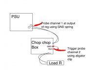
You need to get into the habit of hand-drawing a schematic showing the PSU board (as a box), the ChopBox (as a box), the inductive load resistor, the six wires which interconnect these, the two scope ground clips, and the two scope probe tips.
You know how these are configured. Your readers don't.
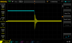
Everything I see here, leads me to the tentative conclusion that the MOSFET-switched inductive wirewound load resistor, is resonating with a capacitance that is connected to the resistor's positive terminal (the +12V power supply buss).
Post597 picture 5 (leading edge of blue gate waveform, 100ns/div) shows that when the MOSFET turns on, the ring a ding ding switches LOW. Just like the bottom end of the resistor-inductor.
Post597 pictures 8 and 10 (falling edge of blue gate waveform, 500ns/div and 200 ns/div) shows that when the MOSFET turns off, the ring a ding ding switches HIGH. Just like the bottom end of the resistor-inductor.
In my opinion, Post598 picture 2 is powerfully indicative. The blue gate waveform follows a classical Miller Effect waveshape. Gate waveform falls until Vgs becomes low enough for the drain voltage to rise ... and then the Miller Effect shunts all further gate current through the CGD capacitance, pegging the gate voltage at a constant plateau. (MOSFET datasheets show this too). Then when the drain voltage has risen most of the way, the gate current resumes discharging the MOSFET gate. The gate quickly drops, the MOSFET cuts off abruptly, and the ring a ding ding switches HIGH. Just like the bottom end of the resistor-inductor.
It's not the slow dI/dt of the drain current during Miller effect dwell time (when the gate is pegged at its plateau value and the drain current decreases slowly) which initiates ringing. No, it's the faster dI/dt when the gate snaps off. Smells like V = L*dI/dt stimulus to me.
I think you will probably want to step back and use probeA to verify/certify/prove that probeB's ground is quiet. Then the other three permutations.
You could start thinking about possible experiments whose goal is to get an idea of the capacitance of the resonant circuit. Knowing its value will probably help you pinpoint its origin. Helpful math: ringing frequency1 is proportional to 1/sqrt(capacitance1) and ringing frequency2 is proportional to 1/sqrt(capacitnace2). If ringing frequency changes by a factor of X then you know that capacitance has changed by a factor of (X*X), namely X squared.
Or you could scheme a way to solder together fifteen carbon composition, noninductive, 3 watt resistors, to get a single 45 watt noninductive resistor. Maybe one of your vendors already sells noninductive power resistors. etc.
You know how these are configured. Your readers don't.
Everything I see here, leads me to the tentative conclusion that the MOSFET-switched inductive wirewound load resistor, is resonating with a capacitance that is connected to the resistor's positive terminal (the +12V power supply buss).
Post597 picture 5 (leading edge of blue gate waveform, 100ns/div) shows that when the MOSFET turns on, the ring a ding ding switches LOW. Just like the bottom end of the resistor-inductor.
Post597 pictures 8 and 10 (falling edge of blue gate waveform, 500ns/div and 200 ns/div) shows that when the MOSFET turns off, the ring a ding ding switches HIGH. Just like the bottom end of the resistor-inductor.
In my opinion, Post598 picture 2 is powerfully indicative. The blue gate waveform follows a classical Miller Effect waveshape. Gate waveform falls until Vgs becomes low enough for the drain voltage to rise ... and then the Miller Effect shunts all further gate current through the CGD capacitance, pegging the gate voltage at a constant plateau. (MOSFET datasheets show this too). Then when the drain voltage has risen most of the way, the gate current resumes discharging the MOSFET gate. The gate quickly drops, the MOSFET cuts off abruptly, and the ring a ding ding switches HIGH. Just like the bottom end of the resistor-inductor.
It's not the slow dI/dt of the drain current during Miller effect dwell time (when the gate is pegged at its plateau value and the drain current decreases slowly) which initiates ringing. No, it's the faster dI/dt when the gate snaps off. Smells like V = L*dI/dt stimulus to me.
I think you will probably want to step back and use probeA to verify/certify/prove that probeB's ground is quiet. Then the other three permutations.
You could start thinking about possible experiments whose goal is to get an idea of the capacitance of the resonant circuit. Knowing its value will probably help you pinpoint its origin. Helpful math: ringing frequency1 is proportional to 1/sqrt(capacitance1) and ringing frequency2 is proportional to 1/sqrt(capacitnace2). If ringing frequency changes by a factor of X then you know that capacitance has changed by a factor of (X*X), namely X squared.
Or you could scheme a way to solder together fifteen carbon composition, noninductive, 3 watt resistors, to get a single 45 watt noninductive resistor. Maybe one of your vendors already sells noninductive power resistors. etc.
You need to get into the habit of hand-drawing a schematic showing the PSU board (as a box), the ChopBox (as a box), the inductive load resistor, the six wires which interconnect these, the two scope ground clips, and the two scope probe tips.
You know how these are configured. Your readers don't.
Fair comment. Sketch and photo attached.
I need more time to reflect on your other comments. Thanks.
(I would not expect my cheap Chinese eBay load resistors to be non-inductive and, as you can see from the pic, the wiring isn't minimal.)
Attachments
- Status
- Not open for further replies.
- Home
- Amplifiers
- Power Supplies
- Adventures with 5A regulated voltage circuits