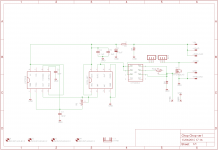
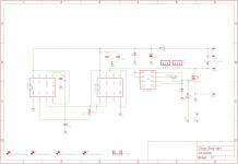
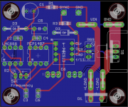
FWIW I decided to spend an hour or so laying out a small (5x5cm) board for the chop chop circuit. I added a dipswitch to be able to opt-in a trim resistor for the MOSFET gate and / or a cap from drain to gate. It is still powered by the supply under test. I added protection diodes for the supply to the LMC555 and MCP1407 and MOSFET gate. Images of first draft attached. Any comments/suggestions welcome.
Attachments
Yikes! D1 is on the wrong side of the series resistor. If VIN > Vzener then Infinity amperes will flow in the zener. This protects the rest of the circuit but only until the zener melts. If you move D1 so it is in parallel with C4, now only (Vin - Vzener)/R1 amperes flow.
You might also consider using an LM7809 series pass voltage regulator instead. This bumps up the component count from 2 (zener, R1) to 3 (7809, input cap, 1.5K load resistor to guarantee 6mA min). I'll bet your MOSFET's Rdson is plenty low with a Vgs of "only" 9 volts.
Or you might consider using a 9V battery. The fewer wires between PSU_under_test and chopbox and BigLoadResistor, the less thinking and circuit analysis you have to do when you see the oscillatory ringing. Hmmm, is the inductance of the Vsupply wire significant? Must I model it? Hmmm
edit- maybe your load resistor is inductive or maybe the wires to it are inductive. maybe this might create a flyback pulse when the MOSFET switches off. maybe you might want flyback protection. as I recall, Elvee's chopbox used a super high VDS rated MOSFET and a rather high voltage MOV lightning arrestor to ground, to protect against flyback without polluting the supply under test.
Last edited:
Oops. I shuffled the series resistor and filter cap around at the last minute and missed shifting D1 also.
I was thinking moving to a battery supply would make sense. I still need to decide on the values of R1 and C1. The LMC555 and MCP1407 only need about 300uA total so R1 can be quite large but the largest I have sitting in my spare parts pile is 8.2K. And the lowest value cap I have lying around is a 16SEPC220MD. If this has above average leakage presumably it will just weigh on battery life and that's about all.
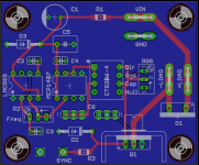
In the iteration above, the load and preload are coupled to the chop chop board. Easy to connect but perhaps, as you say, excess wiring. I guess it makes sense to simply manage a preload across the terminals of the psu board although I'm not sure the net wiring length is lower.
This is the purpose of the varistor? I was just reading about these and need to think how to size one for this application.
I note Elvee also has a resistor between his circuit and the sync probe connection point, presumably as another protection element. I think I will add an SMD 4k7 as I have a few spare.
Thanks
I was thinking moving to a battery supply would make sense. I still need to decide on the values of R1 and C1. The LMC555 and MCP1407 only need about 300uA total so R1 can be quite large but the largest I have sitting in my spare parts pile is 8.2K. And the lowest value cap I have lying around is a 16SEPC220MD. If this has above average leakage presumably it will just weigh on battery life and that's about all.
In the iteration above, the load and preload are coupled to the chop chop board. Easy to connect but perhaps, as you say, excess wiring. I guess it makes sense to simply manage a preload across the terminals of the psu board although I'm not sure the net wiring length is lower.
a rather high voltage MOV lightning arrestor to ground
This is the purpose of the varistor? I was just reading about these and need to think how to size one for this application.
I note Elvee also has a resistor between his circuit and the sync probe connection point, presumably as another protection element. I think I will add an SMD 4k7 as I have a few spare.
Thanks
You could explore TVS diodes to ground as alternative flyback pulse swallowers, they seem to be optimized for incredibly fast turn on and incredibly high peak currents, at the expense of loose tolerances. Mouser part number 576-SA33A might be a good place to start looking ... it will take you to the TVS subsection of the site, where you can browse all their offerings. Guaranteed 54V clamping, guaranteed 9.6A surge current ought to be plenty good enough to protect a 100V MOSFET driving 5A into an inductive load.
This MOSFET gives similar performance at VGS>6 but has greater VDSmax, so it can tolerate a bigger inductive flyback pulse.
Or you could use the standard Ultrafast Diode To Supply circuit design and just perform careful PCB layout such that the flyback current loop is small and tight, whereas the current path from load resistor back upstream to PSU board is longer and less enticing. {like a Kelvin connection} Either PMEG45A10EP (SMD) or BYV10X-600 (thru hole) would be good diode choices.
Or put on belt and braces & do both. High VDS MOSFET and low Vclamp diode across the load resistor. Now you don't have to ramp up to speed on Transient Voltage Suppressors or Metal Oxide Varistors.
_
Attachments
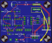
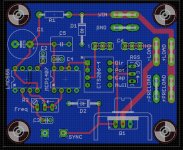
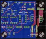
Revised version. I added a GND polygon on the top layer from FET to I/O gnd. This is in addition to the path on the bottom gnd pour. I'm wondering if it is better to reduce the size of the bottom pour (pull the right boundary left) so that the top polygon is the only path from FET to I/O gnd. (The bottom gnd pour has thermals but the smaller top polygon does not.)
EDIT: position 4 of the dipswitch might even be used as an on/off switch...
EDIT: position 4 of the dipswitch might even be used as an on/off switch...
Attachments
Last edited:
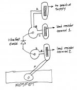
I suggest you give serious thought to creating a PCB "footprint" of a one-terminal component called "BussBar001". This goes on the non-component side of the board between the FET source and the GND connector blade. It is a pad .195" wide and just the right length to almost reach from FET source pad to GND pad. Then wire them all together with a big fat trace / GND fill.
Why is it .195" wide? So you can solder a great big ole bohunker piece of copper braid to it. The copper braid is .145" wide, giving .025 surround (margin for placement error) on either side. During fabrication, apply much much solder and turn that braid from copper colored to solder colored. BFMI. (brute force massive ignorance)
Here is a Mouser link for the copper braid: (Chemtronix rosin core desoldering braid)
NOW calculate the impedance from FET ground to I/O ground. Is it less than 200 microohms?
Do you want to put another BussBar002 on the topside as well? Be sure to avoid the heatsink.
Suggest you use the 4th dipswitch to add another 100nF in parallel with timing capacitor C3, reducing the oscillator frequency by 11X, similar to Elvee's original Chopp Boxxx.
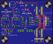
Clever. Revision attached. I added a large SMD pad for the braid. (It doesn't show up well in the image but you can just see the hash markings.) By my calculations there doesn't need to be one of the top layer (I will use 2oz copper) to get below 200uR but I may as well pour a thick copper trace to match on top as it's free.
Attachments

That layout is very nice! Good idea to connect to the FET before making the plane. It appears there is room in the vicinity of LMC555 pin 8, to install a two-pin header which connects or disconnects +Supply from the 555 and thus enables/disables oscillation. Pin1 and Pin2 form an SPST swich. When a shorting plug is installed, the switch is closed.
Another place for a supply-disconnect header that you may like even better is just below R1, which would remove +supply from everything. This connection guarantees that the MCP1407's output certainly is not high when the header is pulled and the thing is supposed to shut off. Wanna 100K across D2 for even more peace of mind?
Just choose a place that is NOT between the bypass caps and the MCP1407 supply pins -- that's a 6 ampere current path.
Some people would advise you to paint the bottom edge of the heatsink with nail polish, just to provide another layer of protection against shorting to the top layer of the PCB after the heatsink eventually rubs away the soldermask insulation. You could also apply one sided foam tape to the PCB, to act as both an electrical insulator and a mechanical barrier + vibration damper. Maybe like THIS, sorry for the USA product link.
Finally I recommend you double check your calculations for the dynamic power dissipation of charging and discharging the MOSFET's gate once per cycle of the oscillator. MOSFET datasheets now specify total gate charge Qgtot, and by the definition of current {amperes = coulombs per second}, Iavg = (Qgtot * frequency). That is likely to be the single largest component of the summation which gives you the total current drawn from your zener diode shunt regulator. The worst case max current occurs at the max oscillation frequency. Maybe your series resistor value is drastically, embarrassingly too small. Or too big. Or maybe not.
ok I will look supply disconnect options. Regarding the heat sink, it is actually elevated some 4mm above the PCB. The bottom of the heat sink is level with the bottom of the case of the pass transistor but the latter is elevated due to widening of its pins near the case.
Oops! If f=1/(1.4 x R2 x C3) with C6 switched out and the low end of range of my 100k trim resistor is 2 Ohms max (if this is the definition of end resistance) then the frequency could be absurdly high. With a max Qgtot of 41nC then Iavg could be as high as 1.46A (?) Feels like I should have a series resistor with R2, say 68k, to set a sensible upper level for the switching frequency? (As well as correcting R1) Or have I screwed up my maths...
Finally I recommend you double check your calculations for the dynamic power dissipation of charging and discharging the MOSFET's gate once per cycle of the oscillator. MOSFET datasheets now specify total gate charge Qgtot, and by the definition of current {amperes = coulombs per second}, Iavg = (Qgtot * frequency). That is likely to be the single largest component of the summation which gives you the total current drawn from your zener diode shunt regulator. The worst case max current occurs at the max oscillation frequency. Maybe your series resistor value is drastically, embarrassingly too small. Or too big. Or maybe not.
Oops! If f=1/(1.4 x R2 x C3) with C6 switched out and the low end of range of my 100k trim resistor is 2 Ohms max (if this is the definition of end resistance) then the frequency could be absurdly high. With a max Qgtot of 41nC then Iavg could be as high as 1.46A (?) Feels like I should have a series resistor with R2, say 68k, to set a sensible upper level for the switching frequency? (As well as correcting R1) Or have I screwed up my maths...
LTSPICE component library called "misc" includes a 555.
Although if you have no plans to sell or give away your chopbox you could follow the ancient wisdom laid down by ancient comedian Henny Youngman.
Although if you have no plans to sell or give away your chopbox you could follow the ancient wisdom laid down by ancient comedian Henny Youngman.
I says to the doctor, I says "Doctor, it hurts when I do this!" Doctor says, "Don't do that"
Thanks for the heads up re the generic 555. A quick model matches my calculations so at least I didn't screw up the simple arithmetic. Perhaps I am missing something else. I note Elvee's box has frequency adjustable between 10Hz ~1KHz. 168K, with 10nF C3, in this box would mean a frequency of ~425Hz while 68K => ~1.05KHz. With the 100n cap switched in the lower frequency bound is ~39Hz. Cap the frequency of oscillation at levels like 1.05KHz and Iavg = (Qgtot * frequency) is always manageable.
Circuit designers learn to live with tradeoffs. "Help me Obi-Wan Kenobi, you're my only hope" imposters, depend on others to make decisions for them.
It occurs to me that if you plan to connect the opamp's +supply pin, to the series pass transistor output (12 volts), then you may need to start looking for a 3 volt opamp with plenty of common mode input range and common mode output range -- to use in your 3.3V PSU board. You might or might not want a third different opamp type for your 5.0V PSU board.
Circuit designers learn to live with tradeoffs. "Help me Obi-Wan Kenobi, you're my only hope" imposters, depend on others to make decisions for them.
Fair. I have not ben able to focus on this for the last three days but I have been thinking about one more addition to the circuit. It would be good to know if the supply voltage kicks higher, e.g. due to the PSU under test FET blowing, and the 12V zener diode is called upon to protect the circuit. I was thinking about adding an LED in series with the 12V zener protection diode. When the zener is forced to conduct, the LED lights up and I know I have a problem. I guess the 'problem' with this is that the circuit's Vs is then only protected at Zener voltage plus the forward voltage of the LED. However, I understand that a typical 3mm red LED such as this one has a Vf of 2V. Therefore Vs is protected at 14V versus an absolute maximum supply voltage for the LMC555 of 15V.
It occurs to me that if you plan to connect the opamp's +supply pin, to the series pass transistor output (12 volts), then you may need to start looking for a 3 volt opamp with plenty of common mode input range and common mode output range -- to use in your 3.3V PSU board. You might or might not want a third different opamp type for your 5.0V PSU board.
Hi. I don't follow you. Yes, I was planning to supply the other two PSU boards with 12V (from the 12V PSU board) for their respective op amp Vs and Vref circuit portions. Only the 12V PSU board op amp will be supplied from board's own series pass transistor.
Phew. Thanks.
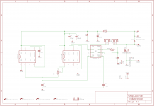
Revised chop chop box board and schematic attached. I have settled on a value of 1400 Ohms for R4 and 1100 Ohms for R1. My rationale was as follows. R4 implies a maximum oscillation frequency of 51KHz (50x the upper bound of Elvee's box). Surely this will be more than enough. If I ever need more I can adjust the board's component values.
I then solved for R1. If R4 is 1400 implying a max freq of oscillation of 51kHz then Iavg = Qgtot x freq = 2.1mA when maximum Qgtot is 41nC. So the circuit will need at least 2.1mA. To provide for headroom I used 3mA and solved for R1 when Vin is at its lowest 3.3V, i.e. R1=1100 Ohms.
If the PSU-under-test FET blows and Vin goes to 25V then I believe things will still be inside the ability of D3 (1.3W) and its series LED (30mA max DC fwd current) to protect the chop chop board.
Attachments
- Status
- Not open for further replies.
- Home
- Amplifiers
- Power Supplies
- Adventures with 5A regulated voltage circuits