I think you will probably want to step back and use probeA to verify/certify/prove that probeB's ground is quiet. Then the other three permutations.
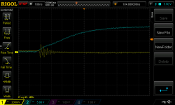
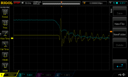
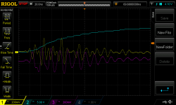
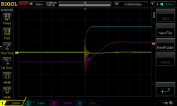
I didn't get a chance to spend much time on this tonight, but I did do the following. I disconnected the load resistor and I connected probe A (channel 1 in the above schematic) to GND A on the chop chop box. (GND A does appear to be the quietest.) The GND alligator clip of the probe was connected to the GND of the reg output at the output caps. When the chop chop box is switched on I see the waveforms in the pics below. The first two are with the chop chop box gate waveform switched to 'hard' (no gate stopper resistor) and the second two are when Rgs is engaged to soften the gate voltage rise/fall. Measured this way, the ground of the chop chop box doesn't appear to be hugely quiet without a gate stopper resistor engaged. So perhaps some of the load ringing witnessed is due to parasitic inductance interacting with the gate capacitance of the chop chop box's gate capacitance.
I'm still trying to get my hear around the 9th pic in post 597. The snap was taken with the measurement probe held in mid air (neither GND nor probe connected).
Or you could scheme a way to solder together fifteen carbon composition, noninductive, 3 watt resistors, to get a single 45 watt noninductive resistor. Maybe one of your vendors already sells noninductive power resistors. etc.
I don't need this to be perfect. I would just like a bit of confidence that I can use this tool to refine the choice between a Zobel network or gate stopper resistor on the regulator pass transistor and any necessary op amp compensation. (Currently I have a 47R gate stopper installed rather than the Zobel option.)
Attachments

Last edited:
Fair comment. Sketch and photo attached.
I need more time to reflect on your other comments. Thanks.
(I would not expect my cheap Chinese eBay load resistors to be non-inductive and, as you can see from the pic, the wiring isn't minimal.)
How long are the wires between the various parts? Fast switching current into wires will automagically generate ringing due to dI/dT in inductive connections.
Not sure it is possible, but you probably want to connect the load very close to the supply, and the chop chop box to the same terminals, ideally zero connection length.
Jan
In short, too long. Between the reg and the chop chop box is about 5 or so inches. The leads on the load resistors are long, around 13 inches.
I know this test setup isn't perfect. As noted previously, I doubt my load resistors are non-inductive also.
I'm just hoping it is a useful tool for refining some of the reg components. I need to reflect on the measurements taken thus far...
Post 601 should have read "parasitic inductance interacting with the gate capacitance of the chop chop box's pass transistor."
In short, too long. Between the reg and the chop chop box is about 5 or so inches. The leads on the load resistors are long, around 13 inches.
I know this test setup isn't perfect. As noted previously, I doubt my load resistors are non-inductive also.
I'm just hoping it is a useful tool for refining some of the reg components. I need to reflect on the measurements taken thus far...
Post 601 should have read "parasitic inductance interacting with the gate capacitance of the chop chop box's pass transistor."
Its really the basic question: what am I measuring, the DUT or the test set?
Not an easy situation to be in.
I respect your drive and stamina; I'm sure you'll get to the bottom of this!
Jan
One of the challenges I find as a newbie is identifying that which I can ignore, knowing my test setup has imperfections. I'd love to just ignore what I see in the first few 100ns, test a couple of other op amp compensation permutations as they model better line rejection and move on. 🙂
I think Mark deserves the gold medal for stamina...
I think Mark deserves the gold medal for stamina...
Yes Mark certainly has been with you all the way!
I still think that you should slow down the rise/fall times of the current jumps to get them closer to what you would expect from a audio supply with a margin. That way, you can actually measure your supply because the test system is an order of magnitude faster than the DUT, thus is outside the equation.
Jan
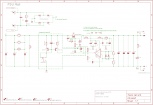
FWIW I also took a look at a modified board layout (and somewhat simpler circuit) to power the op amp and Vref from Vout. I corrected my previous LM4040 pin configuration error and improved a few things such as enlarging certain solder pads, shifting a few things slightly etc.
Power for the op amp and Vref comes either from Vout via R12, a zero Ohm jumper, in the case of the 12V rail or via the solder pads marked +12Vin/GND from the 12V rail for the 5V and 3V3 boards (R12 omitted in these latter cases). (R13 acts as a jumper when the voltage stepper components Z2 and C7 are omitted for the 5V and 3V3 rails.)
I took note of Mark's suggestion in post 469 re 2W or greater Zener diodes but needed to reduce the size with a surface mount option. I was thinking a Vishay BZG03C18TR with a via to the lower layer ground plane.
Attachments
Last edited:
Hi TransmissionAcquitain, in my experience of asking for assistance here you are much better off opening a new thread. You'll likely get more help and possibly attract more people to your project. (Unfortunately I am not the one to answer your questions.)
Everything I see here, leads me to the tentative conclusion that the MOSFET-switched inductive wirewound load resistor, is resonating with a capacitance that is connected to the resistor's positive terminal (the +12V power supply buss).
.....
In my opinion, Post598 picture 2 is powerfully indicative. ....
It's not the slow dI/dt of the drain current during Miller effect dwell time (when the gate is pegged at its plateau value and the drain current decreases slowly) which initiates ringing. No, it's the faster dI/dt when the gate snaps off. Smells like V = L*dI/dt stimulus to me.
.....
You could start thinking about possible experiments whose goal is to get an idea of the capacitance of the resonant circuit. Knowing its value will probably help you pinpoint its origin. Helpful math: ringing frequency1 is proportional to 1/sqrt(capacitance1) and ringing frequency2 is proportional to 1/sqrt(capacitnace2). If ringing frequency changes by a factor of X then you know that capacitance has changed by a factor of (X*X), namely X squared.
Or you could scheme a way to solder together fifteen carbon composition, noninductive, 3 watt resistors, to get a single 45 watt noninductive resistor. Maybe one of your vendors already sells noninductive power resistors. etc.
Mark, thanks for all this. I think I follow your logic.
FWIW I spent some time looking at modelling changes to output capacitance and its affect on transient response and stability. I had previously been adding additional output capacitance while looking at modelled output impedance but I take on board Peufeu's comment of some time ago that targeting regulator output impedance at levels below subsequent wiring resistance is only for glory. In contrast, reducing output capacitance (and using caps with smaller pin pitch to have lower ESL) can improve modelled transient response, lowering the amplitude of the error swing and quickening settling time (so long as there's enough to retain stability).
This analysis led me to remove another of the 470u output caps (i.e. to go from 2x470u to a single 470u). Modelling suggests reducing it further (220u 3.5mm pitch) and if I do another version of the board I will allow for the option of a 2.5mm pitch cap (rather than 3.5mm). 220u or even 150u seems to be enough output capacitance and the 150u can come in 2.5mm pitch.
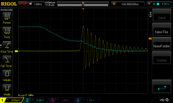
I took transient measurements before and after halving the output capacitance. All measurements had the chop chop box gatestopper resistor engaged to about 90 Ohms. (I'm not sure if Jan would prefer an even slower rise/fall gate stimulus time.) The first two pics below are before (2x470u output caps) while the second two are after (1x470u output cap). As best as I can determine, the ringing frequency didn't change. I get circa 27.5MHz for the trailing-stimulus waveform. (I tried also using my scope's freq function but it produced a very different number. I need to read the manual.) The amplitude of the ringing actually increased - in contrast to modelling projections.
All this leads me, perhaps belatedly, to the somewhat unfortunate conclusion - and to your last point (and Jan's comments regarding the complexity of the task at hand) - that this test setup isn't going to help me fine-tune regulator components. All I am going to get is confirmation that the reg doesn't break into oscillation and deductions such as that which you made above (and thanks very much for this) that observed ringing is most likely due to inductance-capacitance interaction rather than too low regulator phase margin. Maybe at some later point I will build a better, non-inductive, load resistor and revisit this, but for now I think I will just have to 'fly by modelling' so long as I can draw the tentative conclusions you did.
With a 47R gate stopper resistor and a simple 47p Miller compensation capacitor around the op amp my modelling produces the attached line rejection. The gate stopper kills some of the high frequency performance, but I'm in two minds about trying to test the Zobel alternative given all the above.
Am I just chickening out?
Attachments
Last edited:
Perhaps the most telling indicator that the load resistor is a cause of the problem is that I can greatly change the dampening exhibited by placing my hand on the resistor. (They were advertised as "non-inductive" but came from China so who knows.)
Last edited:
I recommend you connect both scope probes' ground clips to the same point, so you don't have current running from one ground clip, up through that probe cable to the scope, through the scope mainframe, and back out the other probe cable to the other ground clip.
I suggest you hope for the best and connect both ground clips to the ground point that is electrically nearest the error opamp -- perhaps the ground lead of its supply bypass capacitors.
Hope for the best -- let us hope you'll still get a clean enough rising or falling edge on the FET gate waveform (set it for fastest edge rate), to reliably and repeatably trigger the scope. If so then you are in good shape to connect the other scope probe tip to the series pass transistor output. If you don't see ringing THERE, you don't have feedback loop instability. And now you can proceed to monkey with gate resistors, no gate resistors, gate-to-drain RC networks, etc. -- all the while observing the actual feedback loop itself and not the horrible artefacts of the LC resonant circuit in the chop box.
BTW it sounds to me like the resonant circuit's capacitance is ACROSS the wirewound resistor, i.e., self capacitance. You could toss in a quick 10nF* capacitor across it and see what happens. We expect (a) the oscillation frequency reduces {freq is proportional to 1/sqrt(Cold+Cnew)}, and also (b) the ringing Q increases, i.e., the ringing damping factor zeta decreases, i.e., the ringing dies out more slowly {zeta is proportional to 1/sqrt(Cold+Cnew)}
*Fword if I know the self capacitance of your wirewound resistor. Maybe 1nF is a better value. Or maybe 100nF. You want something big enough to change the frequency by ~2X but not by 200X and not by 1.0002X. Fword if I know what that capacitance value might be. Experiment and learn.
_
Attachments
Last edited:
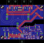
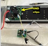
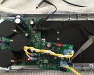
I placed a pin at the position marked in the first pic attached. It's the closest place to the op amp at which I can connect the probe GND clips. Pic of setup attached also. I was able to trigger the scope without issue. Unfortunately the ringing is still very much evident.
Pics:
1. Board join placement
2. Test setup photo
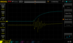
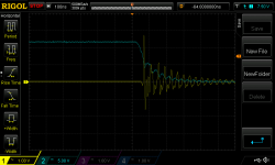
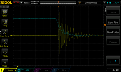
3. Leading edge at reg pass transistor output
4. Trailing edge at reg pass transistor output
5. Trailing edge at reg pass transistor output with load resistor wires twisted
6. Chop chop box switched to soft edge 1
7. Chop chop box switched to soft edge 2
8-10. Measurements taken at op amp output (chop chop box set to hard edge)
Will now take a look at placing a 10nF cap across the load resistor...
Pics:
1. Board join placement
2. Test setup photo
3. Leading edge at reg pass transistor output
4. Trailing edge at reg pass transistor output
5. Trailing edge at reg pass transistor output with load resistor wires twisted
6. Chop chop box switched to soft edge 1
7. Chop chop box switched to soft edge 2
8-10. Measurements taken at op amp output (chop chop box set to hard edge)
Will now take a look at placing a 10nF cap across the load resistor...
Attachments
-
 Op amp trailing.png34.7 KB · Views: 80
 -
 Op amp leading.png35 KB · Views: 91
 -
 Op amp overview.png40.4 KB · Views: 83
 -
 Soft2.png38.1 KB · Views: 84
 -
 Soft1.png34.7 KB · Views: 79
 -
 Trailing twist.png34.6 KB · Views: 87
 -
 Trailing.png37.4 KB · Views: 139
 -
 Leading.png36.4 KB · Views: 145
 -
 Test setup.jpg146.5 KB · Views: 149
 -
 Board.png408.8 KB · Views: 147
BTW it sounds to me like the resonant circuit's capacitance is ACROSS the wirewound resistor, i.e., self capacitance. You could toss in a quick 10nF* capacitor across it and see what happens. We expect (a) the oscillation frequency reduces {freq is proportional to 1/sqrt(Cold+Cnew)}, and also (b) the ringing Q increases, i.e., the ringing damping factor zeta decreases, i.e., the ringing dies out more slowly {zeta is proportional to 1/sqrt(Cold+Cnew)}
Two pics. First WITH 100nF across the load resistor terminals. Second, WITHOUT. The difference with 10nF was hard to discern.
There's a lot of noise in the first pic and as a result estimating the frequency appears challenging. The main peaks do suggest to me a lower frequency. The ringing certainly dies out more slowly.
Does anyone have experience with Arcol low/non-inductive resistors?
Attachments
It looks like you did luck out; the trigger waveform in blue does have a nice region of low contamination where you can reliably and repeatably trigger.
Since you have a four channel scope, why not try to see whether the opamp output is (a) causing, or (b) fighting against, the ring-a-ding-ding?
Chan1 (trigger) on FET gate
Chan2 on Opamp output pin
Chan3 on series pass transistor output (source) pin
If Chan2 is lower magnitude than Chan3, or (ideally) if Chan2 is upside down from Chan3, then the opamp is fighting against the yuck behavior. And we applaud.
You could also consider a previous poster's suggestion, to make the stimulus current step smaller, and then rely upon the system's linearity. If it's marginally stable for a 2000 mA current step, it's marginally stable for a 50 mA current step too. But maybe the smaller dI/dt will generate less yuck on the wires between the chop box and the PSU. Certainly you will be able to fabricate a 240 ohm, 1 watt, noninductive resistor from four 1Ks or eight 2Ks, in parallel.
I wonder whether you could reduce the wirelength to one inch, if you used twisted solid core wires to go between the PSU and the chop box? Solid core would support the weight of the chop box PCB directly above the PSU PCB. Less wirelength means better signal integrity.
Dunno quite what to make of the 100nF experiment; damn thing refuses to give unambiguous results.
Since you have a four channel scope, why not try to see whether the opamp output is (a) causing, or (b) fighting against, the ring-a-ding-ding?
Chan1 (trigger) on FET gate
Chan2 on Opamp output pin
Chan3 on series pass transistor output (source) pin
If Chan2 is lower magnitude than Chan3, or (ideally) if Chan2 is upside down from Chan3, then the opamp is fighting against the yuck behavior. And we applaud.
You could also consider a previous poster's suggestion, to make the stimulus current step smaller, and then rely upon the system's linearity. If it's marginally stable for a 2000 mA current step, it's marginally stable for a 50 mA current step too. But maybe the smaller dI/dt will generate less yuck on the wires between the chop box and the PSU. Certainly you will be able to fabricate a 240 ohm, 1 watt, noninductive resistor from four 1Ks or eight 2Ks, in parallel.
I wonder whether you could reduce the wirelength to one inch, if you used twisted solid core wires to go between the PSU and the chop box? Solid core would support the weight of the chop box PCB directly above the PSU PCB. Less wirelength means better signal integrity.
Hi. Thanks. I reduced the wiring length between the chop chop box and reg output considerably. I also deployed three scope probes as you suggested:
Ch 1 yellow: At reg pass transistor source (clinging to the protection diode construction).
Ch 2 blue/trigger: sync pin of chop chop box
Ch 3 magenta: hand placed at reg's op amp output
All ground clips clinging to the same place as before.
First pic is unfortunately unlikely to generate applause. 🙁 Second pic is a closer look at same. Last 3 pics look at the leading edge.
Unfortunately my stock of through hole resistors is limited and so I will have to buy some (luckily RS Online has free delivery regardless of order amount albeit less stock options). What sort of resistor composition would be best suited to such an application? Carbon as you previously mentioned?
Attachments

Those pictures are disappointing; I was hoping for a smoking gun that said the feedback loop was obviously stable.
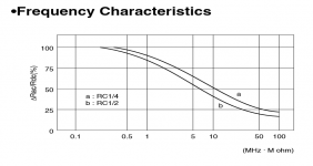
UK RS_Online sells some very nice 0.5 watt carbon composition resistors called Arcol RCC whose (datasheet) contains a wonderful figure; I've attached it below.
You'll notice that the "AC resistance" (impedance) of these resistors DOES NOT RISE with frequency. In other words, they are not inductive. That's just what you want. I'll let other readers tell you how to extract the end-to-end capacitance of these resistors (71 femto farads!) from the plot -- it's negligibly small.
I suggest you put four 1K ohm, 1/2 watt resistors in parallel, with the leads bent and soldered in such a way as to make snug connection to the FastOn female spade jacks. Or, since RS forces you to buy in multiples of 25, you could also put eight 2K ohm resistors in parallel. But this might be a large and unwieldy knob, cumbersome to work with, compared to the four resistor assembly.
Or you might favor a different final resistance value rather than 250 ohms.
(link to RS Online sales Webpage)
_
Attachments
Last edited:
Many thanks - again.
I guess I could also see if I can manage 8x1K for double the load or some other permutation (e.g. 4 x 470R or 6 x 750R). Would a higher load (but with good resistors) not be better if still well within the power rating of the resistors?
I guess I could also see if I can manage 8x1K for double the load or some other permutation (e.g. 4 x 470R or 6 x 750R). Would a higher load (but with good resistors) not be better if still well within the power rating of the resistors?
Last edited:
Well we are also worried about the tens of thousands of microohms of resistance in the ground network on the main PCB, which might confound the results a bit. So a smaller current step might be better but how low is low enough?
Sure, make up a 250 ohm load and a 125 ohm load out of the 25 resistors in the package. Maybe even buy a second package of 25 resistors and make a yet-lower valued noninductive resistor. But the goal is to send a current step big enough to stimulate the feedback loop while also small enough not to produce huge oscillatory ringing in the parasitic Ls and Cs. My intuition is that 100mA ought to be plenty, especially when you've removed all but one of the output electrolytics.
Sure, make up a 250 ohm load and a 125 ohm load out of the 25 resistors in the package. Maybe even buy a second package of 25 resistors and make a yet-lower valued noninductive resistor. But the goal is to send a current step big enough to stimulate the feedback loop while also small enough not to produce huge oscillatory ringing in the parasitic Ls and Cs. My intuition is that 100mA ought to be plenty, especially when you've removed all but one of the output electrolytics.
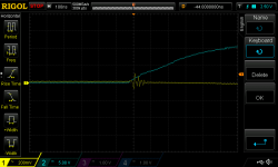
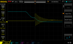
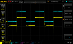
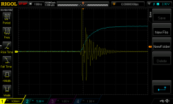
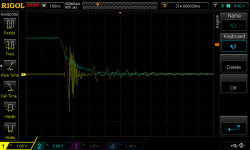
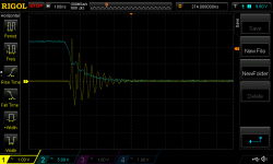
Ok here are some tests with a 100mA step - 4x470R resistors in parallel, bundled into two Faston connectors.
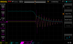
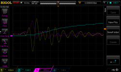
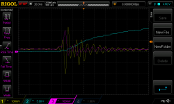
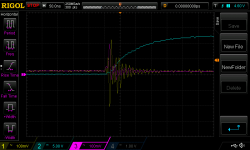
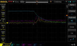
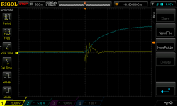
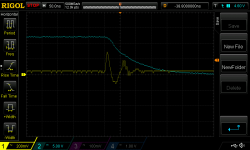
The first 4 pics are taken with an identical setup (apart from the revised load) as before: 3 scope probe GND clips connected to the same spot; cyan trace is stimulus (chop chop gate waveform), yellow is reg output at pass transistor source and magenta is op amp output. All tests are with a hard edge to the stimulus waveform.
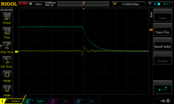
Pic 1 is trailing edge. (Note changes to scales.)
Pic 2, 3 and 4 looking at the leading edge.
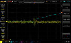
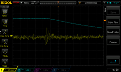
Pic 5, 6 and 7 were taken at the output cap of the reg with the GND spring on the probe. First 2 are leading edge while the third is, obviously, trailing. These last three are starting to look closer to what I see in LTspice as the reg reacts with the output cap ESL except as regards the amplitude of the ringing. Pic 8 is from my LTspice model (trailing edge reaction to 0.1A step in 20ns).
The first 4 pics are taken with an identical setup (apart from the revised load) as before: 3 scope probe GND clips connected to the same spot; cyan trace is stimulus (chop chop gate waveform), yellow is reg output at pass transistor source and magenta is op amp output. All tests are with a hard edge to the stimulus waveform.
Pic 1 is trailing edge. (Note changes to scales.)
Pic 2, 3 and 4 looking at the leading edge.
Pic 5, 6 and 7 were taken at the output cap of the reg with the GND spring on the probe. First 2 are leading edge while the third is, obviously, trailing. These last three are starting to look closer to what I see in LTspice as the reg reacts with the output cap ESL except as regards the amplitude of the ringing. Pic 8 is from my LTspice model (trailing edge reaction to 0.1A step in 20ns).
Attachments


Last edited:
Better! Have you experimented with 32x waveform averaging (Rigol "Acquire" menu)? It might get rid of some of the digital quantization jaggies as seen at the far left of picture #1.
- Status
- Not open for further replies.
- Home
- Amplifiers
- Power Supplies
- Adventures with 5A regulated voltage circuits