I haven't but I will. I've been forced to 'clear all my [expletive] off the dining room table for a bit.' Will try to take a look tomorrow. Should I stick to the 3 probe configuration (with ground clips at the same spot)? It's rather cumbersome, but I am surprised at the very significant differences in the yellow waveform in the first 4 pics vs the next 3.
You don't want the ground clips at two different places - that will lead to current loops through the probe cables' ground wires. But sure, experiment away. Connect the common-scope-ground at different spots and see what there is to be seen, maybe a Eureka awaits.
I wonder whether you can get a decent display with a single channel arrangement, both viewing and triggering from Channel 1, if you probe the regulator output exactly at the spot where it enters the feedback loop? That's the place where the regulator is trying to make the voltage fixed and constant, independent of load. But ... is it?
I wonder whether you can get a decent display with a single channel arrangement, both viewing and triggering from Channel 1, if you probe the regulator output exactly at the spot where it enters the feedback loop? That's the place where the regulator is trying to make the voltage fixed and constant, independent of load. But ... is it?
Attachments
It would be good to know if the supply voltage kicks higher, e.g. due to the PSU under test FET blowing, and the 12V zener diode is called upon to protect the circuit. I was thinking about adding an LED in series with the 12V zener protection diode. When the zener is forced to conduct, the LED lights up and I know I have a problem. I guess the 'problem' with this is that the circuit's Vs is then only protected at Zener voltage plus the forward voltage of the LED. However, I understand that a typical 3mm red LED such as this one has a Vf of 2V. Therefore Vs is protected at 14V versus an absolute maximum supply voltage for the LMC555 of 15V.
Hmm. This didn't work.
My wife went out for a bit so I dragged everything out again. Near the end of my tests using the Rigol's averaging, I slipped with the probe and it caught the +ve output pin of the reg while ungrounded. A couple of sparks. The FET blew. Yet with 25V going to the chop chop box the LED didn't light.
Well I am pretty sure that was when the FET blew, but without the indicator I can't be absolutely certain. So I will do the tests again.
FET replaced. Back to 12V output. Should have bought them in bulk. Grrhh!
PS: it doesn't take long for the 0.5W 470R load resistors to get very hot! I pretty much have to set things up, switch the chop chop box on, grab a wide scope shot (I have been using Single mode), switch off the chop chop box and then play around with resolution and saving images.
Alrighty. All pics with 32 averaging this time.
I tried a single probe with placement as suggested in post 622 (using the probe GND spring) but I could not get readily select the leading vs trailing stimulus edge and so returned to using two probes, both with their alligator GND clips attached to the pin near the op amp GND.
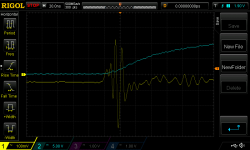
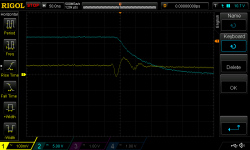
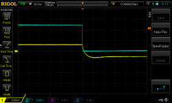
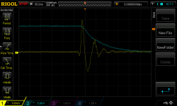
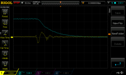
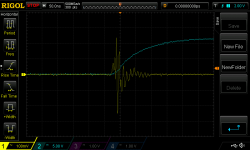
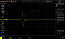
The first pic, leading edge of stimulus, is probed at the high side of Rx (Vout). Pic 2 is probed at the output pin of the reg (Vout).
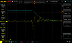
Third pic, trailing edge stimulus, at the high side of Rx (Vout). Fourth at the output pin of the reg (Vout).
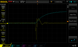
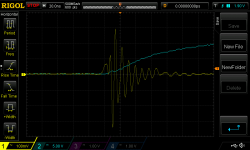
Last few pics are probing the op amp output (ahead of the level shift).
None of this looks particularly encouraging to me. A comparison of the third and fourth pics is particularly bothering me. Both probe Vout. Yet probing near the output cap produces ringing with significantly larger amplitude and, it appears to me, opposite polarity (if it is appropriate to use that term) versus probing at the high side of Rx. 😕
I tried a single probe with placement as suggested in post 622 (using the probe GND spring) but I could not get readily select the leading vs trailing stimulus edge and so returned to using two probes, both with their alligator GND clips attached to the pin near the op amp GND.
The first pic, leading edge of stimulus, is probed at the high side of Rx (Vout). Pic 2 is probed at the output pin of the reg (Vout).
Third pic, trailing edge stimulus, at the high side of Rx (Vout). Fourth at the output pin of the reg (Vout).
Last few pics are probing the op amp output (ahead of the level shift).
None of this looks particularly encouraging to me. A comparison of the third and fourth pics is particularly bothering me. Both probe Vout. Yet probing near the output cap produces ringing with significantly larger amplitude and, it appears to me, opposite polarity (if it is appropriate to use that term) versus probing at the high side of Rx. 😕
Attachments

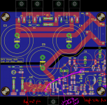
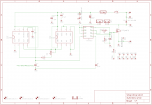
For completeness, here is a pic of the board furthered annotated to show how I have jumpered things to power the op amp and Vref from Vout. R6 and R8 are removed, as is Z1. I have soldered a short piece of wire from an output cap pad to the +12Vin entry point at R15 (which is 499R). As previously mentioned, I have removed all but one of the 470uF 25V output caps. (All other components remain in place even though there are some that are redundant with the aforementioned changes.)
Attachments
Your instruments are telling you that there is some kind of high frequency ringing on Vout -- and you're tying Vout straight to the supply pin of the opamp. How do you feel about that? Do you think it might be worthwhile to splice a 100 ohm resistor in the middle of that magenta jumper wire in post #625? Just to eliminate that from the wish-I-had-tried-X list?
Now might be the time to give up on this line of investigation if you're completely out of ideas. Declare the chop box to be a mysterious distraction that ultimately did not help very much.
Maybe you'll want to try Jan D's idea: find a way to load the supply with a sinusoidal current whose amplitude and frequency are variable. Like maybe a class-A audio amplifier driving a load resistor. Your signal generator driving the amplifier's input, lets you vary the amplitude and frequency.
Or maybe you just want to hook the sucker up to its final digital computer load, attach probes, and see what happens.
If I were you, I would buy some thru-hole parts and recreate the entire VREF network and the entire opamp power supply network from the original design, on a solderless breadboard. I would figure out what went wrong {which you already know: your real life PJFET's Idss was far far lower than what your current mirror needed, to adequately bias the zener and the IC voltage reference} and figure out how to fix it. You may have to purchase some SOT23-to-thruhole adapter boards (link 1) , (link 2) , (link 3) , (link 4) if it turns out that lots more PJFETs are available in SMT than in thru-hole. Or you may wish to use an NJFET, with appropriate pinscramble, instead.
Then with a working breadboard showing me that it is indeed possible to get the original conception of VREF + OAsupply to work, I would solder the appropriate SMT parts onto the final PCB. But that's just me.
Your instruments are telling you that there is some kind of high frequency ringing on Vout -- and you're tying Vout straight to the supply pin of the opamp. How do you feel about that?
Not good. It was on my mind when I added post 625. It's interesting to think that any reg will have a at least a kick to Vout when stimulated with a transient and that any reg with the op amp and Vref driven from Vout will be susceptible to this issue - just in a lesser way if Vout responds modestly to the transient.
Do you think it might be worthwhile to splice a 100 ohm resistor in the middle of that magenta jumper wire in post #625? Just to eliminate that from the wish-I-had-tried-X list?
I can do that but it's not clear to me why it might help.
Maybe you'll want to try Jan D's idea: find a way to load the supply with a sinusoidal current whose amplitude and frequency are variable. Like maybe a class-A audio amplifier driving a load resistor. Your signal generator driving the amplifier's input, lets you vary the amplitude and frequency.
I'm reluctant to start messing with my Krell amps...
Or maybe you just want to hook the sucker up to its final digital computer load, attach probes, and see what happens.
This requires me to complete the other 2 voltage rails. I wasn't going to do this until I had confidence even the 12V worked. And I'm not there yet...
If I were you, I would buy some thru-hole parts and recreate the entire VREF network and the entire opamp power supply network from the original design, on a solderless breadboard. I would figure out what went wrong {which you already know: your real life PJFET's Idss was far far lower than what your current mirror needed, to adequately bias the zener and the IC voltage reference} and figure out how to fix it. You may have to purchase some SOT23-to-thruhole adapter boards (link 1) , (link 2) , (link 3) , (link 4) if it turns out that lots more PJFETs are available in SMT than in thru-hole. Or you may wish to use an NJFET, with appropriate pinscramble, instead.
Then with a working breadboard showing me that it is indeed possible to get the original conception of VREF + OAsupply to work, I would solder the appropriate SMT parts onto the final PCB. But that's just me.
I need to go back over this but I recall that even though the JFET Idss was somewhat lower than expected it did all work...
PS did you by chance have any thoughts regarding the apparent conflict between pics 3 and 4 in post 624?
Last edited:
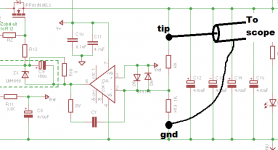
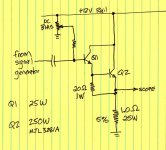
One way to build a suitable class-A amplifier is shown below. The signal generator sets the frequency and the amplitude. Then while looking at the scope, you dial the DC bias potentiometer to get a sinewave that falls almost all the way to ground but not quite (so you don't clip). Ohm's law, I = V/R and since R=1.0, the arithmetic is simple. Your scope displays current-in-the-resistor which is also current-drawn-from-plus-12-volts.
I strongly suspect a clever person could figure out how to do the same thing using a dirt-cheap eBay audio power amplifier. Signal generator goes into audio amp input. Amp output drives your +12V power supply's output through a 4 ohm load resistor and a coupling capacitor. Work out the details, done. Little or no soldering.
Or seek Jan D's advice since he is the originator of the idea.
_
Attachments
Thanks. I need to have a think about what I am going to do. I'm inclined to revert back to the 'powered by Vin' setup (as it was) for now.
(FYI I don't have a signal generator - I'm regretting not taking that option with the scope.)
In the interim, I probed Vref...
(FYI I don't have a signal generator - I'm regretting not taking that option with the scope.)
In the interim, I probed Vref...
Attachments
Last edited:
I worry that we should not believe those VREF plots. You're probing directly across the pins of a high quality capacitor so the dV/dt shown on the plots corresponds to an enormous current I, which seems ~ impossible.
Are you saying that C8 (220uF 16V) should prevent such swings in the Vref voltage? FWIW the attached shows where I probed.
A novice thinking out loud after a glass of wine... What else might cause what I see in the scope, which mimics rather well what I see at the output of the reg? If not a change in Vref voltage then doesn't it have to be a change in the ref GND? And if it mimics what I see at the output caps then that to is perhaps the GND being thumped...
I shifted both GND clips to GND A on the chop chop box. Whether I probe Vout at the output cap, the high side of Rx or GND of the reg board, I get the same image in the scope. Doesn't seem right to me...
Attachments

Electrolytic capacitor C8 is expected to follow the capacitor equation, I = C * dV/dt.
Post 629 shows VREF moving 450 millivolts in 5 nsec. C8 has got VREF on its positive terminal and GND on its negative terminal... about 7 mm distance on the groundplane from your scope's GND clip. Just about as tightly coupled as you could hope for.
If C8 = 47uF then I = (4.7E-5) * (4.5E-1) / (5.0E-9) = 4,200 amperes. Seems wrong.
I think you may have asked a very important question: what ELSE could make my oscilloscope show these waveforms? I don't know the answer at this moment. Take some time to ponder and reflect and cogitate. It may be a Eureka.
I still think this is a measurement issue...either scope user (me) error, scope limitations (?) or chop chop box/test setup limitations i.e. GDN loops or such....but I am the least smart or experienced guy in the room.
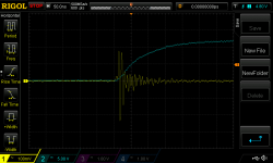
I decided to probe the GND pins on the chop chop box. I started with both alligator clips attached to GND A of the chop chop box. Channel 2 pegged to Sync; Channel 1 probing each of the GND points A to E on the box with the probe point.
For each of B thru E I get the same image - Pic 1. Not a clean GND.
For GND A, same technique, I get the second image. Here I am effectively probing the Channel 1's own alligator clip. Better but still far from clean.
(I then snapped a pic while the Channel 1 alligator clip was attached but the probe was held in the air. Third image; note the change in scale.)
Next, I removed the Channel 1 clip, attached the GND spring and probed GND A again. So here the spring and probe tip are both on the GND A pin, just a few millimetres apart. Third image; note the change in scale.
Last, I removed the alligator clip and 'peg clip' from Channel 2 and performed the previous probe of GND A but now with both probes using GND springs. (For this last test I forgot to engage averaging.) Pic 5.
So...I get a nice gate voltage waveform, with reference to GND A on the chop chop box, but any other GND point on the chop chop box with reference to GND A is a mess....
Whether I probe Vout at the output cap, the high side of Rx or GND of the reg board, I get the same image in the scope.
I decided to probe the GND pins on the chop chop box. I started with both alligator clips attached to GND A of the chop chop box. Channel 2 pegged to Sync; Channel 1 probing each of the GND points A to E on the box with the probe point.
For each of B thru E I get the same image - Pic 1. Not a clean GND.
For GND A, same technique, I get the second image. Here I am effectively probing the Channel 1's own alligator clip. Better but still far from clean.
(I then snapped a pic while the Channel 1 alligator clip was attached but the probe was held in the air. Third image; note the change in scale.)
Next, I removed the Channel 1 clip, attached the GND spring and probed GND A again. So here the spring and probe tip are both on the GND A pin, just a few millimetres apart. Third image; note the change in scale.
Last, I removed the alligator clip and 'peg clip' from Channel 2 and performed the previous probe of GND A but now with both probes using GND springs. (For this last test I forgot to engage averaging.) Pic 5.
So...I get a nice gate voltage waveform, with reference to GND A on the chop chop box, but any other GND point on the chop chop box with reference to GND A is a mess....
Attachments


Mark, I think you are on to something here. That ringing seems not to jive with the waveform risetime.
What else is there in the circuit that DOES have fast risetime? Wasn't there a 555 in it somewhere? Could the 555 ground currents end up on the scope ground? Just grasping at straws here.
Jan
What else is there in the circuit that DOES have fast risetime? Wasn't there a 555 in it somewhere? Could the 555 ground currents end up on the scope ground? Just grasping at straws here.
Jan
Maybe 555 pins 4 & 8 NEED some really effective HF local decoupling.
What is fitted?
1407 pins 1 & 8 have C5 as decoupling. How local is this located?
3 GND pins on U1&2. Where do these go?
What is fitted?
1407 pins 1 & 8 have C5 as decoupling. How local is this located?
3 GND pins on U1&2. Where do these go?
Last edited:
PCB layout shown in post #597. In the layout you can see that LMC555 pin 8 is bypassed by C4 and C5 which are ~5mm north. LMC555 pin4 is not a power supply pin; rather, it is the ResetBar logic signal input and in this design it is tied to logic-one.
As an aside, the last few posts make me wonder if a Vout-powered typology wouldn't benefit from a reasonably-sized cap between Vout and Vin to the op amp to reduce the op amp supply's exposure to transient effects on Vout (much like Vref is by C8 in this reg). I note that the Jung/Didden reg doesn't include this. Is this because there's no issue that would benefit from such cap or would it be expected to compromise start-up?
Was just thinking about you guys this afternoon checking out a HV power supply.
You know I don't believe in testing power supplies with very fast pulses or square waves, because you don't know whether you are testing the switching generator, the wiring, cap load or the power supply. And IF you get a waveform that is ONLY due to power supply performance, what does t tell you? How are you going to judge it?
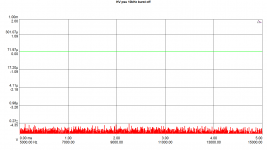
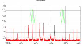
So after some head scratching I came up with this. I tested the power supply with a burst of 10 kHz sine load changes, basically a burst generator connected to a load resistor. I believe that is a realistic test that a supply would have to cope with when powering an analog audio device.
Then I looked at the noise spectrum of the supply output, and of course you see an increase in noise over a band due to the harmonic components of the test signal. The difference between the output noise with and without the burst load tells me how much the supply noise increases due to a certain load and that is something that I can relate to. Still not ideal, but I think a valuable test.
All you need is a function generator and a sound card with an audio test package
Comments invited.
Jan
You know I don't believe in testing power supplies with very fast pulses or square waves, because you don't know whether you are testing the switching generator, the wiring, cap load or the power supply. And IF you get a waveform that is ONLY due to power supply performance, what does t tell you? How are you going to judge it?
So after some head scratching I came up with this. I tested the power supply with a burst of 10 kHz sine load changes, basically a burst generator connected to a load resistor. I believe that is a realistic test that a supply would have to cope with when powering an analog audio device.
Then I looked at the noise spectrum of the supply output, and of course you see an increase in noise over a band due to the harmonic components of the test signal. The difference between the output noise with and without the burst load tells me how much the supply noise increases due to a certain load and that is something that I can relate to. Still not ideal, but I think a valuable test.
All you need is a function generator and a sound card with an audio test package
Comments invited.
Jan
Attachments
- Status
- Not open for further replies.
- Home
- Amplifiers
- Power Supplies
- Adventures with 5A regulated voltage circuits