They are on the current board. But "Vout-driven" is entrenched on the revised - but not yet ordered - board I did. So I can stick with the boards I have, order the Vout-driven revision or merely modify the existing board to deal with the pin-out error and soldering challenges (e.g. tiny pads for C8) and order that.
You are in a box. You can't set the current too high and you can't set the current too low.
Another side to the box. Z3 is a LM4040AIM 5V voltage reference with a 15mA top end to its operating current range and I don't have a slot for a current limiting resistor between it and Q3.
Sure. Or just use a 50mA IDSS device and put a 5Kohm trimmer pot in series with its source (Vgs is no longer zero). Now you can dial the current exactly no matter what IDSS you happen to get; twirl the pot and measure the voltage dropped across the PNP emitter resistor. You can also switch to NJFETs if relaying out the board, since Ntypes are more plentiful and more granular.
Thanks.
FWIW I managed to borrow a friend's "lab" power supply. It's a brute thing and certainly not SOTA. It is, however, meant to be a regulated supply and I used the lowest current capability outlets (6A) in the expectation that they might be the best quality on the thing.
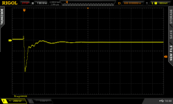
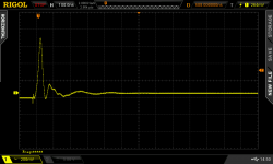
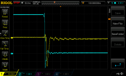
I plugged in my Chop Chop Box with the same length connection leads as I was using to test my regulator circuit. The images below are with the GND alligator clips connected to GND A of the Chop Chop Box (see board image) with the blue trace probing Sync as usual and the yellow trace probing the Chop Chop Box GND E (although probing the other GND points produced similar results).
Rightly or wrongly I take some perverse comfort with respect to my regulator from these. I'm suspicious of my GND plane typology on the Box.
FWIW I managed to borrow a friend's "lab" power supply. It's a brute thing and certainly not SOTA. It is, however, meant to be a regulated supply and I used the lowest current capability outlets (6A) in the expectation that they might be the best quality on the thing.
I plugged in my Chop Chop Box with the same length connection leads as I was using to test my regulator circuit. The images below are with the GND alligator clips connected to GND A of the Chop Chop Box (see board image) with the blue trace probing Sync as usual and the yellow trace probing the Chop Chop Box GND E (although probing the other GND points produced similar results).
Rightly or wrongly I take some perverse comfort with respect to my regulator from these. I'm suspicious of my GND plane typology on the Box.
Attachments

If I were the designer of that power supply under test, I would insist that you connect both scope ground clips to the GND binding post on the front panel of the power supply. That is after all the power supply ground and the supply's noise rejection is defined with respect to this point. Can't get a good sync? Not my problem.
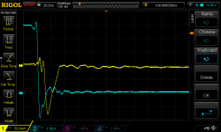
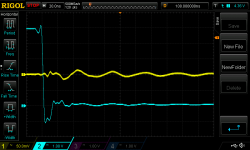
Hi. The waveforms aren't materially different. I shifted both probe GND alligator clips to the -ve terminal of the PSU. The first two pics have the yellow trace still probing GND E on the Chop Chop Box (as above).
The second two pics are probing GND A.
The 5th pic probes the +ve terminal of the PSU. The 6th is the same with the leading edge of the stimulus and is perhaps more easily compared with the 3rd pic of post #652 (albeit with different scale).
As noted above, I would no consider this Nevada PSU SOTA by any means. Perhaps both are cr*p. I thought it interesting to hook up the Chop Chop Box to the only other PSU I can get my hands on currently.
Attachments
Last edited:
Thanks to the nice people in Cupertino California, less than 10 miles from my home, who make (this debugging tool), I had a bit of a minor Eureka.644 pic2 is what you have been wanting to see for 5 weeks. It is here, hallelujah. The only mystery is why the gate node in blue, doesn't show the ringing. Since blue is generated by a 6 ampere driver whose ground is 641 pic1, I expect it to follow the ringing ground.
The gate node in blue doesn't show the ringing because you are filtering it out!
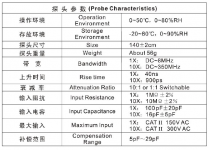
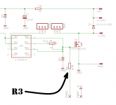
Chop box resistor R3 (see schematic below) combines with the 16 picofarads of the Rigol 300MHz passive probe RP3300, on 10X setting (see specifications below), to form a lowpass filter whose corner frequency is
- f = 1 / (2 * pi * 4.7E3 * 1.6E-11) = 2.1 MHz
_
Attachments
A vineyard which produces some lovely debugging tools... Good stuff.
The rise time of the sync trace is definitely slower than 160ns.
I placed R3 only because I saw the current limiting resistor in Elvee's circuit. It can, of course, be altered but Sync is merely there to trigger the scope.
I'm wondering if I am even thinking about this the right way or merely confusing myself... Am I right in saying that it remains unclear whether it's the GND that's being smacked around or Vout? Pics 4, 5 and 6 of post 652 show Vout (generally) moving inversely with the relative change between the two GNDs. Vout relative to Reg GND goes high just as Chop Chop Box GND A goes low relative to Reg GND (or, inversely, just as Reg GND goes high relative to Chop Chop Box GND A). I'm assuming that in a perfect environment the two GNDs would be the same and, by corollary, if they were then the fluctuation in Vout would not present itself.
(Not that it changes anything, my scope was supplied with the RP2200 probes.)
Last edited:
I myself do not understand what is happening in your set-up nor why it is behaving that way. But now I do understand that it isn't necessary to study or interpret the waveform on the "sync" I/O pin since it is heavily filtered.
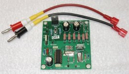
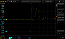
Inspired by posts #665 and #667 in this thread, I built a little Transient Load Test board of my own, photo 1 below. It uses the same STP27N3LH5 MOSFET as SGK's, but the load resistor is on-board to reduce inductance. RLOAD = 6 of (150R 2W) in parallel, giving 25R. Which draws 500mA on a 12V supply.
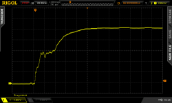
My board includes a 5V regulator IC to limit the VGS of the MOSFET and to power the vanilla CMOS logic chip used as a gate driver and oscillator. Risetime on the MOSFET gate is ~ 80 nsec (photo 2) and fall time on the MOSFET gate is ~ 70 nsec (photo 3). The box runs at 4.5 kHz (photo 4).
I connected the Transient Load tester to a commercially available power supply, the Hantek PPS2320A (sales page). Waveforms at the power supply output terminals are shown in photos 5 and 6. I connected a fixed load of 500 mA on the supply, plus the transient load tester's 500 additional mA, that gets switched on and off, 4500 times a second.
I observe that the Hantek power supply seems to behave better than the Nevada supply in post 667. But they have different load currents, different test cables, etc.
I'll make a new thread for my little tester, so as not to pollute or distract this thread of SGKs.
Attachments

Hi Mark, did you create the other thread? I looked but could not find it. It would be good to understand all the differences in circuit and layout.
I've not done much more with my project over the last week or so while I await the new PSU boards. When they arrive, which shouldn't be too long now, I will prepare the 5V and 3V3 boards.
I've not done much more with my project over the last week or so while I await the new PSU boards. When they arrive, which shouldn't be too long now, I will prepare the 5V and 3V3 boards.
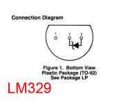
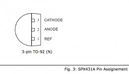
Grrrh. Just found another error in my boards (both old and new). The 12V uses an LM329 as one of the voltage references while I substitute this with an SPX431 in the 5V and 3V3 boards. Same package. Different pin layout. Given ref on the SPX431 was going to be left unconnected anyway, I will just clip this lead off and stuff the two other leads to correctly affix anode and cathode.
Must pay greater attention to detail
Must pay greater attention to detail
Attachments
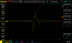
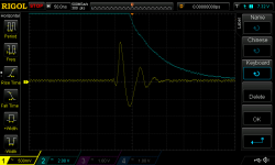
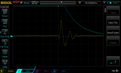
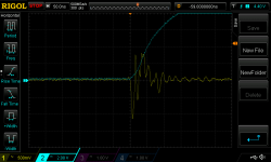
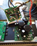
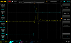
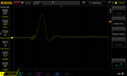
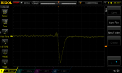
Mark was immensely generous and sent me a package which included boards and parts for his transient load tester. It arrived about an hour ago. To my very pleasant surprise the package also included a fully assembled board set up to load a 12V supply with a pulsing 0.5A load (and with 22 Ohm gatestopper resistors). I couldn't resist connecting it up to my 12V supply and nervously seeing the results - which are somewhat puzzling.
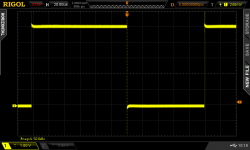
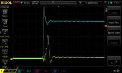
Pic 1 shows the load tester connected to my 12V supply and the trigger probe attached. For this probe I have just used the alligator clip and lead.
Pics 2 and 3 (50s per division and then 20s per division) show the rising edge of load tester's pass transistor gate waveform, turquoise/aqua trace, and the results of probing Vout at the output of the 12V supply under test, yellow trace. The latter was conducted with the probe's GND alligator clip and probe point clip removed and the GND spring attached.
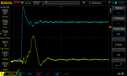
These images are with the scope in Single Mode. Perhaps images taken by stopping the scope when in Normal or Auto Mode are more informative? Pics 4 and 5.
Pics 6-9 are the equivalent but with the trailing edge of the stimulus.
(The last pic is merely with the 'Vout' probe held in mid-air.)
The transient load tester's MOSFET gate rise time and fall time are materially different from those shown in Mark's post here. Much faster rise and fall with significant overshoot.
(Initially I found the relationship between the two traces confusing until I realised the scope trigger attachment point is upstream of the final inverters driving the gate.)
Also, there appears to still be some ringing going on but first I'm wondering about the tester gate rise/fall time which I don't believe should be dependent on the DUT...
PS I used 32 sample averaging
Pic 1 shows the load tester connected to my 12V supply and the trigger probe attached. For this probe I have just used the alligator clip and lead.
Pics 2 and 3 (50s per division and then 20s per division) show the rising edge of load tester's pass transistor gate waveform, turquoise/aqua trace, and the results of probing Vout at the output of the 12V supply under test, yellow trace. The latter was conducted with the probe's GND alligator clip and probe point clip removed and the GND spring attached.
These images are with the scope in Single Mode. Perhaps images taken by stopping the scope when in Normal or Auto Mode are more informative? Pics 4 and 5.
Pics 6-9 are the equivalent but with the trailing edge of the stimulus.
(The last pic is merely with the 'Vout' probe held in mid-air.)
The transient load tester's MOSFET gate rise time and fall time are materially different from those shown in Mark's post here. Much faster rise and fall with significant overshoot.
(Initially I found the relationship between the two traces confusing until I realised the scope trigger attachment point is upstream of the final inverters driving the gate.)
Also, there appears to still be some ringing going on but first I'm wondering about the tester gate rise/fall time which I don't believe should be dependent on the DUT...
PS I used 32 sample averaging
Attachments
-
 NewFile8.png36 KB · Views: 84
 -
 NewFile7.png35.6 KB · Views: 133
 -
 Test setup.jpg184.2 KB · Views: 127
 -
 NewFile9.png34.8 KB · Views: 86
 -
 NewFile10.png38 KB · Views: 81
 -
 NewFile13.png35.7 KB · Views: 80
 -
 NewFile14.png36.1 KB · Views: 79
 -
 NewFile11.png34.7 KB · Views: 85
 -
 NewFile12.png37.4 KB · Views: 80
 -
 NewFile15.png35.8 KB · Views: 78
Last edited:
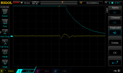
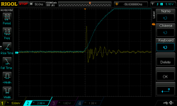
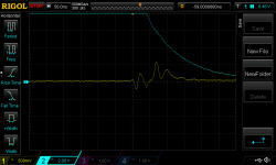
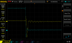
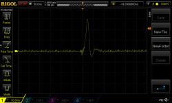
In a fit of great contortion I managed to use GND springs rather than the alligator clips and leads on both the Vout probe and the trigger probe. This cleaned up the gate waveform a bit although the questions above still remain.
100ns, 50ns and 20s per division pics attached.
100ns, 50ns and 20s per division pics attached.
Attachments

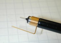
One of the things you will discover after an hour of using a chop chop test board is, the board has got very high dI/dt signals. Even with a groundplane, these dI/dt's manage to couple into any conductor at all, producing M*dI/dt measurement errors (M = mutual inductance). The only thing you can do is keep the M small and thus keep the M*dI/dt small.
This means short wires.
This means short ground wires.
This means short ground wires on your scope probe. Use the short springy clippy ground as depicted in the picture below. You'll know your ground wire is too long if you connect it to PCBground and then put the scope probe right on that ground, and you see any wiggles at all. Ground should be a flatline with no wiggles. If you see wiggles you've got too much M, too much M*dI/dt.
Another thing you will quickly discover is, the "trigger" aka "sync" signal is pretty much useless, because it's relative to the wrong ground. You want to measure the PSU output with respect to the PSU ground and so you want your scope's ground to be the PSU ground. Not the chop box trigger signal's ground.
Another thing you will quickly discover is, you can get along just fine without the trigger signal. Just use a single channel with a single probe, calibrate that probe's overshoot/undershoot on the probe calibrator, connect the shortest possible ground wire, and trigger on the PSU output waveform. Yes if the PSU were perfect then there would be no PSU output waveform and no ability to trigger. Fortunately it's imperfect and a few minutes of jockeying with the scope controls will teach you how. Me, I prefer to hold the probe and springy ground with my right hand, while manipulating the scope trigger controls with my left.
If you have a trustworthy lab assistant, he/she can dial the trigger level while you hold the probe and springy ground with both hands. JUST MAKE SURE TO TELL HIM/HER NEVER TO TOUCH THE "AUTO" BUTTON OR YOU WILL BOTH DIE A SLOW AND PAINFUL DEATH. As you will eventually discover, this will reset the probe coupling to DC (you want AC), the vertical gain to "way too little", the sweep rate to "stupid", the trigger settings to "terrible", and your mood to "foul".
If you have an assistant, you can attempt two channel probing. You hold one probe in each hand and the assistant jockeys with the trigger settings. When you get the picture you want, the assistant hits RUN/STOP (NOT AUTO!) and you can now let go of the probes and save the resultant waveform picture.
_
Attachments
Another thing you will quickly discover is, the "trigger" aka "sync" signal is pretty much useless, because it's relative to the wrong ground. You want to measure the PSU output with respect to the PSU ground and so you want your scope's ground to be the PSU ground. Not the chop box trigger signal's ground.
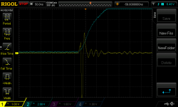
So I understand this properly as I think this is important a great source of confusion... The problem with post 676 is that the scope trigger channel's ground sets the ground for the scope as a whole? In that post I was using the springy thingies, trigger was channel two (turquoise) and its GND spring was on the transient tester GND while the probe probing Vout had its spring on the reg GND.
Another thing you will quickly discover is, you can get along just fine without the trigger signal.
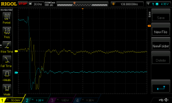
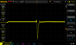
This is a lot easier. 🙂 First 2 pics attached show the transient load tester's MOSFET gate waveform probed in accordance with the guidance you provided here. Looks much more like your results. Second two pics show probing Vout of the regulator board under test (relative to its GND). Doesn't seem too bad...
I'm just not clear as to why what I did in post 676 got everything screwed up. I can see that probing the tester's trigger pin with the GND spring in the GND side socket of C7 doesn't properly show the gate waveform (as does pic 1 and 2) but I am not sure why the yellow probe which is on reg Vout and its GND - just as it was when taking pics 3 and 4 hereto - doesn't provide the same result.
Attachments
Last edited:
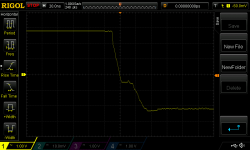
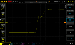
After viewing pictures 3 and 4 of post #678, I now pronounce your 12V PSU board to be free from instability at this one value of DC load current. Try it again with various sized external load resistors, thus various amounts of DC load current, and sleep soundly.
- Connect Rext=infinity, toggle between 0.01A and 0.51A
- Connect Rext=6.0R (>75W), toggle between 2.0A and 2.5A
- Connect Rext=2.66R (>180W), toggle between 4.5A and 5.0A
Last edited:
After viewing pictures 3 and 4 of post #678, I now pronounce your 12V PSU board to be free from instability at this one value of DC load current. Try it again with various sized external load resistors, thus various amounts of DC load current, and sleep soundly.
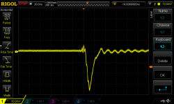
Phew! A step in the right direction. (The current configuration is 'powered from Vout' and a 47R gatestopper for the reg's pass MOSFET.) I guess I am back to adding my large and potentially inductive 200W load resistors. 6in leads are also pretty much a necessity.
I did a quick test with a 6 Ohm 'pre-load' i.e. 2.0A<->2.5A. Ringing creeps in as the load steps up. I'll do more testing in the coming days.
Got it.edit
Many, many thanks for all the help!!
Attachments
- Status
- Not open for further replies.
- Home
- Amplifiers
- Power Supplies
- Adventures with 5A regulated voltage circuits