For I2S output the crystals provide the SAI clock for the MCU which generates the I2S signals (BCK, SD and LRCK). MCK out is divided from the crystal . For I2S input the board acts as a slave.
Can the slaved I2S input be mastered by bit/frameclock signals generated by the I2S output? I mean the standard duplex operation with DAC and ADC running in sync. Thanks.
I was merely trying to give my advice on what I think is the best clock concept for a USB interface. Feel free to disagree and design it the way you want.
Thanks for the advice. I do not disagree with that. However you seem to not fully understand how STM32F7 SAI works. My objective was not to build the best possible USBI2S bridge but to build a STM32F7 based one.
I just made a jtest in REW on the RTX6001, with a loop back connection. I used settings very similar to yours to make it easier to compare (FFT lenght, window, averaging etc.). The result is attached.
Are the DAC and ADC clocked by the same master clock?
Can the slaved I2S input be mastered by bit/frameclock signals generated by the I2S output? I mean the standard duplex operation with DAC and ADC running in sync. Thanks.
That should be possible as both I2S input and output are running on the same SAI. But I have not tried it yet as the I2S input software is still work-in-progress.
Actually syncing is possible even between separate SAIs.
Last edited:
You are correct, I don't know how the STM32F7 SAI works. I just assumed that there is another clock to run the processor and the USB, with audio clocks being separate and selectable. There seems to be 3 crystal oscillators on your design.Thanks for the advice. I do not disagree with that. However you seem to not fully understand how STM32F7 SAI works. My objective was not to build the best possible USBI2S bridge but to build a STM32F7 based one.
Yes, they are clocked by the same master clock. I once made a similar test, where I used two units, one as the generator and one as the analyzer. The result was very similar, if not the same, compared to using one unit in loopback mode. It may have been with a 10 kHz sine wave though, not the jtest.Are the DAC and ADC clocked by the same master clock?
I just made a jtest in REW on the RTX6001, with a loop back connection. I used settings very similar to yours to make it easier to compare (FFT lenght, window, averaging etc.). The result is attached.
This is coherent measurement as should be at best...
Just do the same using two, one as DAC the other as ADC and than may 😱 😀
Hp
The SAI of STM32F7 is certainly very flexible, allowing all modes of operation, including the external clock behind the isolator, IMO. The chip looks like a perfect fit for this feature 🙂 Of course another criterum is quality of the UAC2 device implementation which I have no idea about.
https://www.st.com/content/ccc/reso...nt/translations/en.STM32F7_Peripheral_SAI.pdf
https://www.st.com/content/ccc/reso...nt/translations/en.STM32F7_Peripheral_SAI.pdf
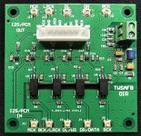
I just assumed that there is another clock to run the processor and the USB, with audio clocks being separate and selectable. There seems to be 3 crystal oscillators on your design.
Actually there are 4 oscillators (25MHz & 32.768kHz for the MCU).
STM32F7 (as probably most Cortex-M MCUs) can generate the I2S clock using PLL. However this results in slight inaccuracy in the frequencies as the PLL is integer based. The "audiophile" approach is to input the audio clock to a GPIO pin which results in accurate frequencies (and possibly lower jitter). The SAI (Serial Audio Interface) uses this audio clock to generate the actual I2S signals (BCK, SD, LRCK and possibly MCK).
I fail to see how placing the audio input clocks outside the isolator would improve jitter in this case as the actual I2S signals will anyhow need to go through an isolator. The MCK may have less jitter but does that really help.
In oversampling devices the conversion is typically clocked by the master clock, I2S is usually "just" for data transport. That's why placing the master clock on the DAC/ADC side of the isolation is the preferred method, if such arrangement is supported.
The SAI of STM32F7 is certainly very flexible, allowing all modes of operation, including the external clock behind the isolator, IMO. The chip looks like a perfect fit for this feature 🙂 Of course another criterum is quality of the UAC2 device implementation which I have no idea about.
The USB implementation of STM32F7 (or F2-H7) is based on Synopsys OTG controller. This is largely (if not totally) undocumented so in that sense the STM32F7 USB is a black-box. The HAL-part is just a thin layer on top of the Synopsys OTG. But so far I have not stumbled on anything seriously bad about the STM32F7 USB implementation. I assume even 768k/32 is possible but I have not yet tried that.
In oversampling devices the conversion is typically clocked by the master clock, I2S is usually "just" for data transport. That's why placing the master clock on the DAC/ADC side of the isolation is the preferred method, if such arrangement is supported.
Now we're talking. If MCK is critical I may need to make a new revision of the board 🙂
I fail to see how placing the audio input clocks outside the isolator would improve jitter in this case as the actual I2S signals will anyhow need to go through an isolator. The MCK may have less jitter but does that really help.
In cases where I2S signal jitter may be a concern, if the master clock is on the dac side of the isolators then the master clock can be used to 'reclock' or 're-synchronize' the I2S signals through a D-Flip Flop buffer. For that to work correctly the master clock frequency needs to be at least twice that of the highest I2S clock frequency (otherwise the flip-flops can act as frequency dividers).
Well, one thing is the OTG controller, another thing is the UAC2 implementation. It's the same in linux - the dwc2/3 Synopsys controllers have drivers (with bugs as everything) and each USB device function (uac2, ethernet, mass storage etc.) has its driver (with another load of issues often related to support of drivers in major OSes).
The Synopsys IP implementations differ in each SoC, the documentation quality differs too. Fortunately dedicated Synopsys engineers with inside know-how actively participate in the kernel mailinglists and constantly review or provide patches for dwc2/3. I have only experience with dwc2 in RPi4 and the dwc2 Synopsys engineer has been extremely helpful with ironing out issues. He does have access to dwc2 IP implementation in the Broadcom SoC, sometimes even sent me fragments of their PDFs.
The Synopsys IP implementations differ in each SoC, the documentation quality differs too. Fortunately dedicated Synopsys engineers with inside know-how actively participate in the kernel mailinglists and constantly review or provide patches for dwc2/3. I have only experience with dwc2 in RPi4 and the dwc2 Synopsys engineer has been extremely helpful with ironing out issues. He does have access to dwc2 IP implementation in the Broadcom SoC, sometimes even sent me fragments of their PDFs.
In cases where I2S signal jitter may be a concern, if the master clock is on the dac side of the isolators then the master clock can be used to 'reclock' or 're-synchronize' the I2S signals through a D-Flip Flop buffer. For that to work correctly the master clock frequency needs to be at least twice that of the highest I2S clock frequency (otherwise the flip-flops can act as frequency dividers).
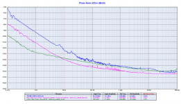
I2S reclocked with master clock after optocouplers and phase noise plot:
- blue line, masterclock
- pink line, reclocked BCK
- green line, reclocked LRCK
Attachments
Well the UAC2 implementation is for the most part mine so the person to blame stares me back in the mirror 😀
I wonder if the "standard" DAC/ADCSs (ESS in sync mode, AKM) are sensitive to I2S jitter when the conversion is clocked by the master clock.
Well the UAC2 implementation is for the most part mine
Great hats off, that's a very complex task. We already talked about it here 🙂
I wonder if the "standard" DAC/ADCSs (ESS in sync mode, AKM) are sensitive to I2S jitter when the conversion is clocked by the master clock.
I don't believe, if you use the Sabre in pure sync mode you need a good master clock only.
Great hats off, that's a very complex task.
I worked 30+ years in IT industry starting with 68000-based VME computers in the 1980s. This STM32F7 UAC2 stuff is probably more complicated that anything I worked with professionally 😀
- Home
- Design & Build
- Equipment & Tools
- ADCs and DACs for audio instrumentation applications