R22 and R23 are actually part of the RIAA network so I'm not quite sure what you mean. You could tweak the 90.9K resistors in the RIAA and make the gate resistors huge and get away with smaller values. Below 20Hz the noise at the output from the input pair is 800nV which is 40M Ohm equivalent resistance.
Folks that need lots of low filtering when playing LP's need to address that some way.
I was thinking more about the gate current noise of the Jfet being magnified by the impedance of the cap/resistor.
I was thinking more about the gate current noise of the Jfet being magnified by the impedance of the cap/resistor.
These FET's typically have femto-amp noise levels. The noise measures as predicted, input/source limited.
Shouldn't C1 be shunting the LEDs?
PS bypassing is left to the user so maybe you say that because there are no caps shown on Vcc?. Any residual noise at that point is common mode and I figure bypassing to ground was maybe better but I don't think it really matters much.
The problem is that any noise on V+ will appear directly across the diode string, and the bias points connected to it. I figured you meant C1 to be across the diode string, but that is also sort of useless, so I am actually not sure why it's even there.
The problem is that any noise on V+ will appear directly across the diode string, and the bias points connected to it. I figured you meant C1 to be across the diode string, but that is also sort of useless, so I am actually not sure why it's even there.
Missed Muntzing opportunity? 🙂
I don't have a single sound card or digital recorder that isn't AC coupled
I could swear mine was AC coupled. Turns out it is not, and I found out the hard way (trying to measure the noise of a 24V regulator). That channel is gone.
To attempt repair I have to dessolder a replacement opamp from another card. It is an odd package, larger than soic8. Need to practice on a dead card before I do the actual surgery.
Please ignore my post above.
(It is AC coupled and is working fine. The free fft software WaveSpectra does strange things every once in a while. Most of the time it works ok though.)
(It is AC coupled and is working fine. The free fft software WaveSpectra does strange things every once in a while. Most of the time it works ok though.)
Any news?
Right... We saw CAD drawings but nothing else.
If there are some Gerbers, maybe someone else can finish it off?
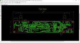
I’d love to get my hands on a through hole pcb (an accompanying psu pcb would be lovely as well).
Is there a final schematic along with gerbers? In the thread there seemed to be some hints to some possible changes (Post #227 ?)
I’m quite eager to try this design and can see what I can do.
Is there a final schematic along with gerbers? In the thread there seemed to be some hints to some possible changes (Post #227 ?)
I’m quite eager to try this design and can see what I can do.
I’d love to get my hands on a through hole pcb (an accompanying psu pcb would be lovely as well).
Is there a final schematic along with gerbers? In the thread there seemed to be some hints to some possible changes (Post #227 ?)
I think I mentioned early on that I just use ExpressPCB but anyone has my blessing to do anything they want with this. IIRC there were some suggestions around using LSK/LSJ parts and readily available Vishay MKP caps both of which should be fine.
I have been asked by a couple of people via PM regarding my protos shown in post #208.
I now have all the matched FETs since December, and is in the process of finishing with soldering.
Test is on my to-do list,
Probably some time in June, if the circuit works as intended.
I am building with a modified circuit and with much higher gain than Scott.
So there might be other issues with DC drift, etc.
We'll see in due course,
Patrick
We'll see in due course,
Patrick
I certainly endorse anything Patrick does, he always takes great care. There must be some kind of psychic connection here 🙂, literally two days ago I started to revisit this (mainly around an open-loop MC head amp). In a week or so I will post some new (un-built) ideas that might interest followers of these minimalist no feedback phono stages.
I continue to be happy with my version and it did perform well at Kevin's, who has a far better listening setup. Patrick is correct the exact gain structure needs to be looked at since the open-loop linearity and noise are connected.
with LSK389 and 300k load one can get 70 dB of gain, MC requires 90 dB at lf, super pair Baxandall Super Pair can help
New Circuits
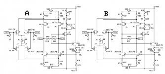
This is a further look at circuits similar to the one in the first post here. Patrick sent me an idea for some changes in an LTSpice file and I stared at it for a while thinking about a MC step up circuit to go with the RIAA pre-amp. I continue to be surprised that the basic topologies in CMOS amps (current mirrors with common mode feedback) don't appear much in discrete JFET circuits. This circuit is, if you will indulge the analogy, close to a solid state version of a 20dB step up transformer but buffered at the input. This circuit is extremely symmetric virtually none of the components appear in the differential signal path but the input devices and the load resistor. Almost every other component's non-idealities appear as common mode errors as well as supply variations. In addition the difference between N and P devices is also cancelled by symmetry. This topology also allows arbitrary cartridge loading.
To walk through the circuit, there are complementary LTP's feeding a folded cascode. This gives a 6db gain boost and 3db noise improvement to the original circuit for free. The current ratio between the input pairs and the cascodes is set simply by R1, this can be used to adjust the gain between two channels making matching of all devices unnecessary. The goal is to have all the devices in the input and cascode run at ~5mA but this is not super critical. R16 sets the common mode voltage (0 ideal) while R4 and R15 are redundant trims for the output offset voltage. At these bias levels the SK170/SJ74 give 0.4nV noise and -90dB THD at 10mV input, the SK146/SJ72 (unobtainium) only improve this to 0.3nV. I have enough NOS Toshiba devices of all these types as well as the equivalent LSK devices to make an apples to apples comparison. So my project over the next few weeks is to build a socketed breadboard and make some measurements.
I never noticed before but the connection of the common mode feedback in version B creates a single ended output. In fact moving the common mode feedback connection alone can make a fully differential or inverting or non-inverting single ended output with no noise and little THD penalty.
At these impedance levels I don't think any buffering is needed. But I can't help but think that the original circuit could be reworked along these lines where the gain resistors are replaced by the RIAA network. This uses more FET's and would have a higher cost.
Attachments
Last edited:
Hi Scott,
There are several Spice models of the 2SK170 / 2SJ74, maybe we are using a different set.
With the given resistor values, I had to use +/- 8.5 Volt power supply to get a current of 3 mA through J1 to J8.
Gain was 11.6 or 21 dB.
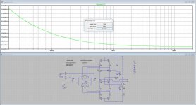
Input Noise from 20 Hz to 20 Khz is 117nV, or an equivalent input noise of 0.83 nV/rtHz, see image below.
There are several Spice models of the 2SK170 / 2SJ74, maybe we are using a different set.
With the given resistor values, I had to use +/- 8.5 Volt power supply to get a current of 3 mA through J1 to J8.
Gain was 11.6 or 21 dB.
Input Noise from 20 Hz to 20 Khz is 117nV, or an equivalent input noise of 0.83 nV/rtHz, see image below.
Attachments
Hi Scott,
There are several Spice models of the 2SK170 / 2SJ74, maybe we are using a different set.
With the given resistor values, I had to use +/- 8.5 Volt power supply to get a current of 3 mA through J1 to J8.
Gain was 11.6 or 21 dB.
Input Noise from 20 Hz to 20 Khz is 117nV, or an equivalent input noise of 0.83 nV/rtHz, see image below.
The supplies are +-15, I meant you adjust R1 to get the currents equal at ~5mA. I put a pot there because that was how you would build it the value is ~40 ohms for my models. I made my own computation of beta and Vto directly off the Toshiba data sheets. I'm using a SPICE deck that Patrick sent me with rearranged devices, I'm simply looking at Vinoise and it seems to be computed in a way that I'm not used to. I'll get back to this because I was thinking originally that I would have to use doubled pairs or the 146/72 devices.
.model 2SJ74 PJF(Beta=56.25m Rs=7.748 Rd=7.748 Betatce=-.5 Lambda=4.464m
+ Vto=-.5164 Vtotc=-2.5m Cgd=85.67p M=.3246 Pb=.3905 Fc=.5
+ Cgs=78.27p Isr=129.8p Nr=2 Is=12.98p N=1 Xti=3 Alpha=10u Vk=100
+ Kf=26.64E-18 Af=1)
.model 2SJ72 PJF(Beta=110.25m Rs=7.748 Rd=7.748 Betatce=-.5 Lambda=4.464m
+ Vto=-.5216 Vtotc=-2.5m Cgd=85.67p M=.3246 Pb=.3905 Fc=.5
+ Cgs=145p Isr=129.8p Nr=2 Is=12.98p N=1 Xti=3 Alpha=10u Vk=100
+ Kf=26.64E-18 Af=1)
.model 2SK170 NJF(Beta=49m Rs=4.151 Rd=4.151 Betatce=-.5 Lambda=1.923m
+ Vto=-.553 Vtotc=-2.5m Cgd=20p M=.3805 Pb=.4746 Fc=.5
+ Cgs=25.48p Isr=84.77p Nr=2 Is=8.477p N=1 Xti=3 Alpha=10u Vk=100
+ Kf=111.3E-18 Af=1)
.model 2SK146 NJF(Beta=76.6m Rs=4.151 Rd=4.151 Betatce=-.5 Lambda=1.923m
+ Vto=-.626 Vtotc=-2.5m Cgd=20p M=.3805 Pb=.4746 Fc=.5
+ Cgs=63p Isr=84.77p Nr=2 Is=8.477p N=1 Xti=3 Alpha=10u Vk=100
+ Kf=111.3E-18 Af=1)
EDIT - Yes I was not expecting the way the AC gain of the input source is treated (this is my first serious use of LTspice). Though I should have known better.
Last edited:
- Home
- Source & Line
- Analogue Source
- A simplified universal differential or single ended phono preamp