This is very interesting. I'm going to play with this and see how it works.
Also, if you don't mind my asking, could you tell me what criteria you used to reject the ten out of twenty-five devices you tested? And any other information you could provide to characterize the differences between devices?
Looking back at my notes, it was actually 30 that I tested. I ran tests at 7 currents ranging from 14ma to 0.01ma. A few had resistances too high or too low across the board. I think I rejected 5 outright as just being too far of outliers (+ or - 20% from the average, some as much as twice or half the average resistance). Honestly, a 5% match is better than almost any standard pot. With a big enough pool of LDRs you could easily get a high percentage of LDR pairs with matches to within 1%.
The formula is just an approximation of the average. Combined with the control response you want and the mechanism you use, you can come up with a way to predict response. For example, I use a dual linear pot to provide voltages to an op-amp acting as a V to I converter to get 0-1.2ma through the LDRs. By adjusting the resistors, I can control the overall response of the LDR network to be approximately ideal log response.
Thanks for the reply.
I got twenty or so LDRs to start with, and have checked only the 20 ma response on them so far. The spec calls for 40 ohms or less at that current. All except one passed that test, but the range of resistances was 37 ohms down to 31 ohms at 20ma, with one outside of tolerance at 58 ohms. The range of 31 to 37 ohms doesn't seem like much until you think of it in terms of current through the device to achieve the standard 40 ohms, it's quite a difference and I suppose that difference will carry through the rest of the curve.
One question I have, which I haven't got data on yet but I'm curious about -- is the shape of the curve consistent between devices with the differences above and below 'average' consistent across the curve for a given device, or does the shape of the curve differ widely between devices? Did you look at that?
The shape is more or less consistent in the samples that I didn't reject. There will be some variation, but that's what matching is for. I found that because of the response, putting more than 5 ma through them was unnecessary. At 6.5ma, the average was 60 ohms and even at 1.5ma, the average response was about 130 ohms. If this represents one end of the response spectrum and In an L pad with another LDR at 170K ohms, the difference of a few ohms is trivial.
I think the formula will be most useful for people with microcontrollers so they can use that rather than a lookup table to determine the current they want through an LDR at any time.
I think the formula will be most useful for people with microcontrollers so they can use that rather than a lookup table to determine the current they want through an LDR at any time.
The shape is more or less consistent in the samples that I didn't reject. There will be some variation, but that's what matching is for. I found that because of the response, putting more than 5 ma through them was unnecessary. At 6.5ma, the average was 60 ohms and even at 1.5ma, the average response was about 130 ohms. If this represents one end of the response spectrum and In an L pad with another LDR at 170K ohms, the difference of a few ohms is trivial.
I think the formula will be most useful for people with microcontrollers so they can use that rather than a lookup table to determine the current they want through an LDR at any time.
My goal is a constant Z 5K pot. At first I was planning to use 150 ohm current limiting resistors for all four devices, but it didn't take long to realize that the series resistor for that value pot starts at 142 ohms for .25dB attenuation and jumps to 280 ohms for .50 attenuation, so decided to use a much larger value resistor for the series devices.
The shunt continues to be problematic, requiring 40 ohms for 42.5dB attenuation at Z=5K. I wonder what attenuation range is adequate to cover any serious listening on virtually any amplifier including high efficiency systems (if you don't worry about low levels that are intended for background music only).
With all the issues of trying to get the lowest resistance from the devices, I'm wondering if using 2 in parallel rather than a single device isn't feasible.
With all the issues of trying to get the lowest resistance from the devices, I'm wondering if using 2 in parallel rather than a single device isn't feasible.
It's perfectly feasible, but costs go up greatly when having to use multiple pairs of matched devices on each leg
Yes the cost will go up, but for those that are bothered by not being able to reach 'zero volume'.
Would you have to double up on all of the devices ?
Surely even just doing one leg of the chain would help.
As for matching, isn't the design Warpo is working on supposed to overcome that problem ?
Anyway, was just a thought I had that could be useful....
Would you have to double up on all of the devices ?
Surely even just doing one leg of the chain would help.
As for matching, isn't the design Warpo is working on supposed to overcome that problem ?
Anyway, was just a thought I had that could be useful....
With all the issues of trying to get the lowest resistance from the devices, I'm wondering if using 2 in parallel rather than a single device isn't feasible.
For my intended pot, the series resistor varies across a fairly narrow range from 142 ohms that ends just below 5K ohm, and doubling would be pointless. It's the shunt resistor that would benefit from a lower resistance. Doubling up the LDR for the 5K pot I'm aiming for would result in a maximum attenuation change from 42.5 dB for a single to 48 dB for a double device (40 ohms for one and 20 ohms for two).
The device itself is a three dollar item, and it's possible the two could work in parallel with only a load-balancing/current limiting resistor for each to equalize current flow if you have the PIC treat the pair as a single device and cailbrate accordingly. However, it may not be that easy, and require the full list of mosfet, capacitor, resistors, plus two additional pins (control & feedback) per added LDR. With my current choice of components, I have no more free control pins available for additional LDR devices.
Last edited:
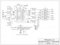
Would you mind posting a schematic for this?
OK, I think all the major kinks are ironed out and I'm ready to share the circuit. Operation of the indicator LED is not yet tested, but the critical LDR sense and control circuits work fine. The only issue there could be is the potential 'ageing' of the LDRs themselves, especially over time. We'll see. A jumper is included to disable the LED if maximum PS stability is desired during normal operation, but still available for programming or to verify PIC operation. In any event, LEDs with current draws as low as 3ma are available, so I don't expect a TO-220 LM317 to be affected at all by LED operation. I can always change LED behavior through programming.
Most recent changes:
1. Added an LED to flash during programming and operation activity, and be steady on when volume is muted (in case someone wants a front-panel indication of that condition).
2. Added R3, R13, and R14 to create a voltage divider to set the ADC +Vref at a point just above where the LDRs reach about 200K resistance. This will allow a finer adjustment of the LED currents within the 10-bit ADC resolution.
3. Changed values of R18 and R20 from 150R to a higher value to better match the actual minimum resistance requirement of the series LDR. Reason is same as for (2.) above.
Time to start programming (sigh, I don't like this part).
Attachments
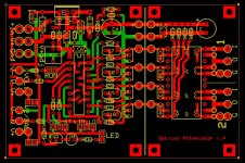
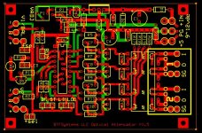
Modified the circuit card layout to achieve several advantages:
1) Card can now be left as one board or split into two sections -- one section houses all of the control circuitry including all of the digital circuitry and power supply, the other houses the LDRs and the input/output solder pads for the audio signal. Requires only six wires to jumper the boards together. This will permit the control circuitry to be located close to the volume and balance pots, and the LDRs to be located immediately adjacent to the input/output jacks.
2) Added additional smoothing capacitor locations close to the LDR current limit resistors.
3) Now possible to split the power supply to allow the LM317 to drive only the control circuitry, and to allow a separate ultra-quiet shunt regulator to supply the LEDs. This can be done either as a single board or split board configuration. I don't believe that this will be necessary at all, but for the ultra-purists in the audience . . .
4) Reduced the number of interconnecting 'nail' locations to eliminate duplication.
5) Changed LDR conductor spacing on carrier from .2" to .1" but carrier size remains the same (24-pin DIL).
6) Made changes to enable V+ selection other than 5.0V -- it appears that 3.7V may be the optimal voltage for this circuit.
Circuit card size remains the same at 2.5" x 4"
Attachments
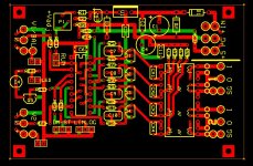
Worked on the circuit card over Christmas, made some significant changes:
1) moved power input/output pads to the rear of the board so that all connections are at the rear, and control pots and indicator LED are at the front.
2) rearranged the voltage regulator circuitry to accomodate 1).
3) separated potentiometer pads to maximum separation so that pots can be soldered directly to board and used to secure the card to front of panel if desired.
I am not certain that the decoupling capacitors are adequate:
220uF 25V & .1uF at power input (C1, C2)
440uF 10V & .1uF at regulator output (C3, C4)
.1uF bypass at control chip power pins (C6)
.1uF bypass at current limiting resistors (C11)
1uF tantalum across each LDR-LED CX1~CX4) (optional)
Separate power supplies for the control chip and the LDRs would be ideal, but I doubt that it will make an audible difference. The control circuit will draw maybe 5ma, and the LDRs will draw maybe a maximum of 40ma total at maximum attenuation. With the pots set in the middle of their ranges, the control voltages are virtually invisible on a scope, they are so small, and the LEDs are drawing negligible current. I've put a 1K resistor (R3) to draw a continuous 5ma to stabilize the regulator. This regulator is going to loaf.
LED current changes during turn on/off affecting the power supply is a concern, but transitions will only happen when the circuit goes in to, or out of, 'mute' mode, so should not be audible.
If anyone has ideas for better decoupling of the control circuit from the supply to the LDRs, I'd be interested to hear your idea.
Attachments
1) The leads of a decoupling capacitor can act like a radiator (antenna) so they should be as short as possible. I don't know if it's possible to "pour copper" for connection of the caps to the ground plane with this program, however.
2) Analog and digital grounds should be kept separate.
etc., etc. See analog devices apnote on grounding and decoupling
2) Analog and digital grounds should be kept separate.
etc., etc. See analog devices apnote on grounding and decoupling
1) The leads of a decoupling capacitor can act like a radiator (antenna) so they should be as short as possible. I don't know if it's possible to "pour copper" for connection of the caps to the ground plane with this program, however.
2) Analog and digital grounds should be kept separate.
etc., etc. See analog devices apnote on grounding and decoupling
The capacitors are all radials, so leads are very short to the foil. Yes, I can do a ground plane on this board, but I'm not sure if it's useful -- the "audio" is restricted to the lower right corner of the board, and the audio grounds (and all audio connections) are very short and completely isolated from the power supply and control circuitry.
I plan to use a wall wart with floating ground so there will never be physical contact between power ground, signal ground, and the chassis.
While the chip is indeed a digital chip and the 'control' signals are digital, when the potentiometers are not moving the control signals are vanishingly small and very occasional -- barely visible on a scope, and they stop at the mosfets Q1~Q4. In reality, there is no digital activity going on outside of the chip itself (the control circuits are mostly "off"). The mosfets act as variable resistors, and the voltages beyond the mosfets to the LEDs is pure DC from the power supply. The only noise that could possibly get there would be through the power delivered through the current limiting resistors to the LEDs.
Having said all that, I could pour a ground plane. I assume that would be around the power supply and control circuits, and not the audio corner, correct? And that ground plane would be connected to the chassis, but not to power ground? Or two ground planes -- one audio and one control circuit -- not connected to each other. (I'll have a look for that application note you mentioned.)
you can see the clock signal with a spectrum analzyser, it's always clocking. Most scopes don't have the sensitivity to see the radiated clock signal. I would suggest pouring copper under the MCU and connect the decoupling cap from the Vdd pin to the plane, using a 100nF ceramic. Keep the analog and signal grounds separate, meeting at only one point. If you have to run an analog signal over the clock or control signal, do so at right angles.
our sensitivity to noise isn't like that of a hydrophone, ekg or seismic instrument so I don't want you to get your knickers too twisted up. Just save some money before sending the design off to PCBExpress.
our sensitivity to noise isn't like that of a hydrophone, ekg or seismic instrument so I don't want you to get your knickers too twisted up. Just save some money before sending the design off to PCBExpress.
you can see the clock signal with a spectrum analzyser, it's always clocking. Most scopes don't have the sensitivity to see the radiated clock signal. I would suggest pouring copper under the MCU and connect the decoupling cap from the Vdd pin to the plane, using a 100nF ceramic. Keep the analog and signal grounds separate, meeting at only one point. If you have to run an analog signal over the clock or control signal, do so at right angles.
our sensitivity to noise isn't like that of a hydrophone, ekg or seismic instrument so I don't want you to get your knickers too twisted up. Just save some money before sending the design off to PCBExpress.
Thanks for the input, I'm going to give this some thought.
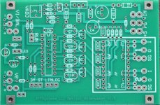
Got my latest boards back with the changes listed above.
Should get the components from digi-key and mouser early next week.
I've decided that 1/8W resistors are too small for comfortable handling, I've redrawn the board to take 1/4W resistors. All else stays the same.
Should get the components from digi-key and mouser early next week.
I've decided that 1/8W resistors are too small for comfortable handling, I've redrawn the board to take 1/4W resistors. All else stays the same.
Attachments
Hi,
the lands around each hole are very narrow. The land is too small for direct contact with the tip of the soldering iron. This makes for more heating of the component while trying to use the component leg to heat the PCB trace.
the lands around each hole are very narrow. The land is too small for direct contact with the tip of the soldering iron. This makes for more heating of the component while trying to use the component leg to heat the PCB trace.
Hi,
the lands around each hole are very narrow. The land is too small for direct contact with the tip of the soldering iron. This makes for more heating of the component while trying to use the component leg to heat the PCB trace.
Hi, Andrew,
I went back and looked at the board, I kinda see what you mean that some of the lands look small. But I have been using this software and this production company for years, and I don't remember experiencing problems soldering. I'll try to be aware and watch for the problem as I solder up this board. It occurs to me to wonder if the land sizes are not intended to be optimal for wave soldering. I never thought of that. To change the land sizes would involve a lot of work changing the component drawings in the software!
There may be some 'optical illusion' going on because the holes for the two IC sockets are oversized (the last board I had made using standard sized holes didn't work for me because I wanted to use machined-pin IC sockets and the pins were too big for the holes). Also, the traces may be unusually wide compared to what you are accustomed to -- I used .04" for signal traces and .06" for power. I've always wondered if there was an optimal trace size for audio signals, but never tried to find an answer to that.
Also, the smallest lands running down the middle of the 20-pin IC outline and attached to the large lands at the edges of the board plus the six on the inside of the 24-pin IC outline are not intended to be soldered to, they are intended to accept the spring-loaded pins of a bed-of-nails board.
The lands other than the IC sockets are all the standard size that come with the component outlines included in the ExpressPCB pcb design software, I haven't changed any of them.
BTW, in order for folks to have the easiest assembling job, I've converted the board from the 1/8W resistors (which are very small) to 1/4W. So the board has changed to the attached design, just a slight rearrangement to accomodate the larger resistors but no increase in overall size. I haven't had one actually made up yet.
Attachments
Got my latest boards back with the changes listed above.
Should get the components from digi-key and mouser early next week.
I've decided that 1/8W resistors are too small for comfortable handling, I've redrawn the board to take 1/4W resistors. All else stays the same.
I remember getting 0.6-Watt resistors through Digikey that were much shorter than 1/4-Watt resistors, but about the same diameter, if that would help.
I remember getting 0.6-Watt resistors through Digikey that were much shorter than 1/4-Watt resistors, but about the same diameter, if that would help.
Well, length of the resistors on this board are not a problem. There are a few places where the 1/4W devices will be cheek-to-jowl in width, but should be OK. I'll stick with the standard 1/4W 1% devices as long as I can. For a while last fall there seemed to be a shortage of these resistors, don't know why, but they're back available now.
- Status
- Not open for further replies.
- Home
- Source & Line
- Analog Line Level
- A precision LED/LDR-based Attenuator