Using USB only forces you to use boosters if you need > 5V. Boosters are active oscillating devices. If you seek the ultimate I would reduce the number of active oscillating components on the board i.e. use no "boosters". This makes you have to leave USB power. If you seek the ultimate, drawing power form an USB device is also typically not optimal as it exists so many bad USB implementations... just my 2€c
//
//
Using USB only forces you to use boosters if you need > 5V. Boosters are active oscillating devices. If you seek the ultimate I would reduce the number of active oscillating components on the board i.e. use no "boosters". This makes you have to leave USB power. If you seek the ultimate, drawing power form an USB device is also typically not optimal as it exists so many bad USB implementations... just my 2€c
//
Of course! This is why we're making the architecture modular so that you could get power from any source you want.
But there won't be any switching regulators on the DAC board. They will be on a separate board.
Any strong opinions on the matter?
We need to keep any switching noise off the power rails. If LDO regulation after the switching power supply helps with noise suppression, then I would use it.
I kept thinking about this and looked for the resistance of connectors like Mil-Max machined carrier sockets. They're in the range of 10mΩ. The ESR of 16SVPK1200M is 12mΩ. And the ESR of EEHZK1E561UP is 20mΩ. Therefore, I am very tempted to solder 4 × EEHZK1E561UP directly on the DAC board and provide sockets for another four capacitors, which could be the 16SVPK1200M or anything else we want. The mating height of the carrier sockets is 2.2mm, which means that mounting capacitors on a 0.8mm thick PCB would only raise them by 3mm.
Chris, I know that you recommended against an extra mezzanine board, but going with this hybrid approach (one soldered and one on a mezzanine, Cf. layout) might create an interesting tradeoff (I really, really like the idea of making it easy to try different capacitors on the final form factor).
What about PCB trace resistance you didn't account for yet? There is also the matter of current loop area. Current flowing in one terminal of a cap back out the other terminal and through the dac chip forms a loop. The area of the loop is an antenna good for picking up magnetic EMI/RFI, and capacitance to the traces at high frequencies provide an antenna to pick up stray electric fields. Also, for caps that are effective at higher frequencies, the added inductance of traces can cause multiple problems.
I guess you could try it both ways and see if there is any perceptible or measurable difference in dac performance. More time, cost, work to do it right to make sure it will work as you hope, and you may already have more problems to solve than you expect. But, hey, its a learning experience, right?
Last edited:
But, hey, its a learning experience, right?
That's right!
"I got 99 problems, but [fear] ain't one."
Last edited:
Could you just put the footprints for both caps down staggered slightly so you could populate either one? It's not the end of the world if you use those headers, but it's not ideal. Probably not an issue with huge electrolytics.
Could you just put the footprints for both caps down staggered slightly so you could populate either one? It's not the end of the world if you use those headers, but it's not ideal. Probably not an issue with huge electrolytics.
That was my intuition as well, but we won't know for sure until we try. And I got really intrigued by these Mil-Max receptacles and pins.
I'm not sure that I understand what you mean regarding staggering. My intuition was also that one set of capacitors should be soldered, with a capacitance as large or larger than the ones mounted on the AKM evaluation board (470μF). That way, in the worst case scenario, we just use these, and we can't be any worse than the evaluation board. And for these, I was planning to use the hybrid capacitors that you recommended, with 560μF capacitance. Then, the removable capacitors mounted on mezzanine boards would be mounted in parallel and would be optional. There, we could put anything we want (either an other 560μF hybrid capacitor, a 1,200μF OS-CON electrolytic, etc.).
Also, I should explain that one of my (very many) goals for this project is to investigate unusual manufacturing techniques, sometimes using uncommon components, with the primary objective of making the architecture as modular as possible. I spent most of my childhood playing with LEGO® bricks, and these left a lasting impression, for better or for worse...
I just meant have room for both cap footprints on the DAC board itself so you could populate either one, but you might be space constrained.
I just meant have room for both cap footprints on the DAC board itself so you could populate either one, but you might be space constrained.
I see! Allow both the soldering of the second capacitor per parallel pair directly on the PCB, or its mounting on a mezzanine board. Yes, we will do that if we can make everything fit.
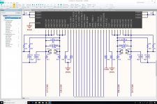
Capacitor on Mezzanine
Here is what the schematic looks like for mounting the larger capacitors on mezzanine boards, in parallel to the 560µF EEHZK1E561UP hybrid capacitors, which will be soldered directly on the DAC board. Each mezzanine board will have a single capacitor and four 4015 receptacles.
Here is what the schematic looks like for mounting the larger capacitors on mezzanine boards, in parallel to the 560µF EEHZK1E561UP hybrid capacitors, which will be soldered directly on the DAC board. Each mezzanine board will have a single capacitor and four 4015 receptacles.
Attachments

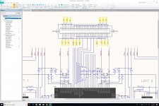
Ground Return Circuits
I have split the ground return circuits on the ERM8 connectors between AVSS and DVSS based on pin proximity. I'm not sure whether this is the conventional way of doing things, but it somehow felt right. Please let me know if I'm missing something.
I have split the ground return circuits on the ERM8 connectors between AVSS and DVSS based on pin proximity. I'm not sure whether this is the conventional way of doing things, but it somehow felt right. Please let me know if I'm missing something.
Attachments
Last edited:
IIRC, on the eval board AKM treated clock signals as digital. More often they may be considered to be high speed analog, but AKM can do it how they want. May matter more what you do at the other end of the ground connections outside the dac module. Loops should be avoided. Grounds used for the dac should only be shared with the power supply module and other modules related to the dac. Other modules for other functions unrelated to the dac could create noise problems if they are on the same power supplies and grounds, especially if the grounding scheme is not carefully thought out to minimize any possibly resulting problems. Once more: hitting performance numbers down around -130dB or below for individual harmonics is not trivial, its getting into an area that can be rather challenging.
I'm sure! If you think some of the ground return pins should be connected to a different ground plane, please let me know.
You will probably need to test the dac with some other modules plugged into the plate to see if they cause interference with each other. Better to do that early on in the testing.
You will probably need to test the dac with some other modules plugged into the plate to see if they cause interference with each other. Better to do that early on in the testing.
Indeed.
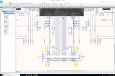
DZFL and DZFR
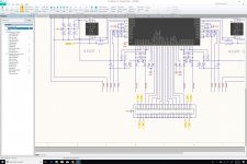
I initially thought that DZFL and DZFR could be hard-wired, but that does not seem to be the case. Instead, we will want to expose these pins as outputs fed back to the MCU. Changes to the schematic have been applied accordingly.
I initially thought that DZFL and DZFR could be hard-wired, but that does not seem to be the case. Instead, we will want to expose these pins as outputs fed back to the MCU. Changes to the schematic have been applied accordingly.
Attachments

Your entire converter should be on one, single, contiguous plane and it's the "analog" plane. I would probably not split the pins like that.
Grounding of Mixes Signal Systems
High frequency currents want to return right under the trace (lowest HF impedance).
Grounding of Mixes Signal Systems
High frequency currents want to return right under the trace (lowest HF impedance).
Your entire converter should be on one, single, contiguous plane and it's the "analog" plane. I would probably not split the pins like that.
Grounding of Mixes Signal Systems
High frequency currents want to return right under the trace (lowest HF impedance).
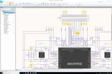
Okay. So all the DVSS circuits will return to this single ground plane? I updated the schematic accordingly.
Attachments
Last edited:
Okay. So all the DVSS circuits will return to this single ground plane? I updated the schematic accordingly.
Yeah, there are no hard and fast rules, but a single plane is probably the safest route to go. Single point grounds and star grounds often do not work well at high frequencies. In my experience, people always worry about high frequency currents, but those return in a very predictable path. It's the low frequency stuff that spreads on the plane. Sometimes you do need a single point connection, but it depends and it's a trade-off.
I would look at what AKM did on their board as a reference. Not that it's perfect or you can't improve on it, but they did get the measured performance they were after. You could also look at the evaluation boards of some of the state-of-the-art non-audio ADCs and DACs to see how they have done it. Those boards typically interface with a mid-range FPGA.
Last edited:
- Home
- Source & Line
- Digital Line Level
- 8 × AK5578EN + 8 × AK4499EQ ADC/DAC Boards