Lots of boards...
In case you're lost, here is a recap of all the boards that could be used to make the full DAC board:
- 1 × Core DAC Board
- 12 × DAC Regulator Boards
- 1 × Clock Board
- 1 × Clock Regulator Board
- 1 × Jung/Didden Super Regulator Board (for VREF)
16 boards in total...
And that's not including the Plate Board with the first stage regulators and the MCU, nor the XLR board with the muting circuits and XLR connectors...
Only CSET, which is the reference filter. The datasheet mentions the effect is negligible for input and output caps due to the PSRR and low output Z. I probably would just use a 22uF X7R myself. Another option that may be better than the tantalum (but larger) is the Al hybrid like I mentioned before:
EEH-ZC1V220R Panasonic Electronic Components | Capacitors | DigiKey
Got it! This hybrid capacitor would not fit on the small regulator boards unfortunately.
Bit behind on this thread, WRT digital decoupling use
22uF or 47uF, mlcc, will usually be Y5V, smallest physical
size possible. These are more effective than paralleling
an electro + .1uF mlcc, by far.
22uF or 47uF, mlcc, will usually be Y5V, smallest physical
size possible. These are more effective than paralleling
an electro + .1uF mlcc, by far.
It took me ages to find these
http://www.hoffmann-hochfrequenz.de/downloads/experiments_with_decoupling_capacitors.pdf
http://www.hoffmann-hochfrequenz.de/downloads/experiments_with_decoupling_capacitors.pdf
Bit behind on this thread, WRT digital decoupling use
22uF or 47uF, mlcc, will usually be Y5V, smallest physical
size possible. These are more effective than paralleling
an electro + .1uF mlcc, by far.
Yes, but that thread is very old. Thank you for linking Gerhard's measurements though.
I would never use a Y5V capacitor under any conditions unless I am trying to shave cents off a product. You just have to look at the Murata SimSurfing page and the graphs to understand why. There have been 22uF and 47uF X5R and X7R caps available for years now in small package sizes (and those are bad enough dielectrics, for me).
The position that was asked about is not digital, it's an internal reference filter cap for the LT3042. Whether an MLCC is best for that or not really depends on your feeling about the piezoelectric tendencies of anything that isn't C0G.
Your point stands, I agree and posted similar a few pages back. The 0.1uF is an urban legend of sorts at this point. I still sprinkle them around in non-critical applications to avoid questions from clients as to why there are no 0.1uF caps.
Last edited:
Reading your comments and the datasheet, I guess we should use a 22µF capacitor on CSET. LDOVR uses the T495C226K025ATE300 tantalum capacitor for CIN. Is it fair to assume that the same capacitor could be used for CSET as well?
Page 17 - Due to its good voltage coefficient in small
case sizes, LTC recommends using Murata’s GJ8 series
ceramic capacitors.
Page 18 - Similarly, due to LT3045’s
ultrahigh PSRR, negligible output noise is generated
using a ceramic input capacitor. Nonetheless, given the
high SET pin impedance, any piezoelectric response
from a ceramic SET pin capacitor generates significant
output noise – peak-to-peak excursions of hundreds of
µVs. However, due to the SET pin capacitor’s high ESR
and ESL tolerance, any non-piezoelectrically responsive
(tantalum, electrolytic, or film) capacitor can be used at
the SET pin – although electrolytic capacitors tend to
have high 1/f noise. In any case, use of a surface mount
capacitor is highly recommended.
Page 19 - In addition to reducing output noise, using a SET pin bypass
capacitor also improves PSRR and transient performance.
Note that any bypass capacitor leakage deteriorates the
LT3045’s DC regulation. Capacitor leakage of even 100nA
is a 0.1% DC error. Therefore, LTC recommends the use
of a good quality low leakage ceramic capacitor.
It took me ages to find these
http://www.hoffmann-hochfrequenz.de/downloads/experiments_with_decoupling_capacitors.pdf
Thanks a lot for these links, super helpful.
Page 17 - Due to its good voltage coefficient in small
case sizes, LTC recommends using Murata’s GJ8 series
ceramic capacitors.
Page 18 - Similarly, due to LT3045’s
ultrahigh PSRR, negligible output noise is generated
using a ceramic input capacitor. Nonetheless, given the
high SET pin impedance, any piezoelectric response
from a ceramic SET pin capacitor generates significant
output noise – peak-to-peak excursions of hundreds of
µVs. However, due to the SET pin capacitor’s high ESR
and ESL tolerance, any non-piezoelectrically responsive
(tantalum, electrolytic, or film) capacitor can be used at
the SET pin – although electrolytic capacitors tend to
have high 1/f noise. In any case, use of a surface mount
capacitor is highly recommended.
Page 19 - In addition to reducing output noise, using a SET pin bypass
capacitor also improves PSRR and transient performance.
Note that any bypass capacitor leakage deteriorates the
LT3045’s DC regulation. Capacitor leakage of even 100nA
is a 0.1% DC error. Therefore, LTC recommends the use
of a good quality low leakage ceramic capacitor.
Indeed. I will try to stick to these as much as possible. I am now combining all the feedback we received on this topic into a summary sheet showing all the regulator modules we need to develop, and which parts they will use. As I am doing that, I am reducing the 6V input down to 5.5V for all the regulators that need to produce 5V (Cf. sheet). That way, we reduce power dissipation by about 50%. This should help quite a lot regarding power management.
In case you're lost, here is a recap of all the boards that could be used to make the full DAC board:
- 1 × Core DAC Board
- 12 × DAC Regulator Boards
- 1 × Clock Board
- 1 × Clock Regulator Board
- 1 × Jung/Didden Super Regulator Board (for VREF)
16 boards in total...
And that's not including the Plate Board with the first stage regulators and the MCU, nor the XLR board with the muting circuits and XLR connectors...
I have been thinking about that design a bit more, and I think that I really like it. It's quite unconventional and will add significant cost to the BOM because of the 852/853 machined pin headers, but it should help reduce implementation risks and improve sound quality. Here is why:
If we were to build a single DAC board with all these components directly mounted on the board, it would be really complex, and any design change of one area might have ripple effects on other parts of the board. Due to my very limited experience (non-existent at this point), we would run a very high risk of running around in circles for a very long time. By breaking the board apart into so many different modules, we can reduce that risk quite a bit.
Another challenge is the complex PCB layout required for the linear regulators. Trying to do such a layout on a 10 or 12-layer PCB would be quite a challenge. But by breaking the board apart into separate modules, we can mimic what Linear is doing on its reference boards, and be sure that our regulator modules will work on their own. This will leave the core DAC board quite simple and manageable as a standalone project.
One learning I gathered from this project so far is that the range of options is limitless, and that what works for a particular DAC chip might not for another. Therefore, the ability to perform a lot of trials and learn from one's errors is paramount. This modular design should make it a lot easier for many more people to participate in such a development process, especially if we end up developing a large collection of regulator modules, clock boards, super regulator boards, etc.
This overall modular approach fits really well with the rest of the project, which is highly modular in nature. Here, we're just introducing modularity at an even finer level of granularity.
Heat Dissipation
Another benefit of the modular architecture we've recently introduced is that it might help with heat dissipation. By mounting all the regulators directly on the DAC board, heat would dissipate throughout the board's PCB, possibly affecting the DAC chip or some other components. By mounting the regulators on separate modules, we avoid that problem, and we can separately optimize heat dissipation for specific regulator modules that might require it most. For such modules, we could even consider making the regulator boards larger and use two or three regulators in parallel, without making any changes to the DAC board.
Also, I have realized that our regulator boards will be mounted from the top of the DAC board where the DAC chip is soldered (in order to avoid any additional vias). Therefore, we are not as vertically constrained as we are on the bottom side (12mm), because the XLR board comes on top, and this one could sit higher (18mm or more). Therefore, we should be able to make our regulator boards much bigger. The 853 connector needs 5.3mm and the 852 needs 4.4mm. This means that we have about 8mm to play with.
Regulator Boards
Here are the regulator boards that we will need for the LT30XX regulators. The capacitors are tantalum for CIN and MLCC for CSET, following what Linear recommendsand what LDOVR is doing. The designators for the capacitors have been adjusted in order to remain simple, but aliases related to the designators used by Linear have been added for reference purposes.
Later on, I will work on a similar list for the LTM804X μModules.
Last edited:
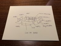
Modular DAC Architecture
Here is what I have in mind regarding the modular architecture for our DAC.
The core DAC board is a 110mm × 35mm board, probably 10 or 12 layers. The AK4499EQ DAC chip sits right in the middle of the top layer. Laying on top of it is a board with four Jung/Didden Super Regulator circuits for the four VREF supplies. This board will be mounted on top of the core DAC board using four sets of 4-pin 852/853 machined pin headers and sockets located very close to their associated pins on the DAC chip. A 16V to 15V LT3042 regulator board (not shown) will lay flat on top of it in order to provide the 15V supply needed by the four AD825 operational amplifiers.
On the bottom of the board, we have two ERM8 connectors (North and South) for digital and analog signals, and two UMPT connectors (East and West, not shown) for power. These connectors allow the DAC board to be mounted on an OTOBUS™ interface board. This board is itself connected to the Plate Board (via two sets of ERM8/ERF8 connectors), which will have the LTM804X µModules and the STM32H743 MCU (with USB interface and Thesycon U-HEAR driver).
Immediately on the North side of the DAC chip are three regulator boards mounted vertically for AVDD (5V), DVDD (1.8V), and TVDD (3.3V). These boards will be mounted in such a way that the traces leading to the respective AVDD (pin 107), DVDD (pin 109), and TVDD (pin 111) pins on the core DAC board are kept as short as possible.
Right behind them is the Clock board, laying flat, on the opposite side of the North-side ERM8 connector. Because the NZ2520SDA crystals are so small (2.5mm × 2mm), it should have no problem fitting all the necessary components. Laying on top of it is an LT3042 regulator board, but with a slightly different form factor than our regular regulator board. The Clock board will use a pair of SMP coaxial connectors with a bullet linking them for the output clock signal, plus a set of 852/853 pin header and socket for power and clock selection. The SMP connector mounted on the board will be very close to the MLCK pin on the DAC chip. The placement of that connector will take priority over the traces for AVDD, DVDD, and TVDD (the four pins are right next to each other on the DAC chip, with DVSS between DVDD and TVDD).
On the West and East sides of the DAC chip are four 5.5V to 5V LT3042 regulator boards mounted vertically for VDDL1, VDDR1, VDDL2, and VDDR2.
Finally, on the far West and far East sides of the core DAC board are two +16V to +15V LT3045 and -16V to -16V LT3094 regulator boards also mounted vertically for MVDD1+, MVDD1-, MVDD2+, and MVDD2-.
This arrangement should leave plenty of room on the core DAC board for all the large capacitors that need to be added, especially on the bottom side of the board (all regulator boards will be mounted on the top side).
The connectors linking the core DAC board to the XLR board to be mounted on top of it have yet to be selected. This selection will be largely influenced by the height of the vertically-mounted regulator boards, which itself will be defined once some PCB layout has been done for them (I'm in Japan right now, away from my EDA workstation).
Nobody has made any comments on this design so far, and I'm really curious to know whether this is a viable approach, or whether this is a dead end (keeping in mind all the constraints that we are trying to deal with of course).
Attachments
Last edited:
On the bottom of the board, we have two ERM8 connectors (North and South) for digital and analog signals, and two UMPT connectors (East and West, not shown) for power. These connectors allow the DAC board to be mounted on an OTOBUS™ interface board. This board is itself connected to the Plate Board (via two sets of ERM8/ERF8 connectors), which will have the LTM804X µModules and the STM32H743 MCU (with USB interface and Thesycon U-HEAR driver).
An alternative approach would consist in putting the ERM8 and UMPT connectors on the same side as the DAC chip, alongside the regulator boards. This would allow us to avoid using vias for all the digital signal and power circuits. And since the shielded versions of the ERF8/ERM8 connectors are available with 16mm mating height, it would still leave plenty of room for the vertically-mounted regulator board.
Also, it means that the Clock board would be on the opposite side of the DAC board (DAC chip at the bottom, Clock board on top), and the use of through-hole SMP connectors would ensure that our clock signal does not go through any via.
This is probably a much better option.
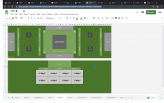
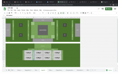
DAC Board Layout
Here is what the layout for the modular DAC board could look like (bottom and top layers). Lighter green areas outline modular boards (regulator modules, super regulator board, and clock board), some vertically-mounted (regulator modules), and some horizontally-mounted (super regulator board, and clock board).
This is crazy, but I kinda like it...
Attachments
Last edited:
Large Capacitors
We've had so many discussions about the large capacitors that I think we should mount them on their own mezzanine board as well, as illustrated here. We would use 850 through-hole machined pin headers to ensure proper connectivity. This design would facilitate the testing of different capacitors and different capacitor combinations. For example, I am wondering how a pair of 1,200µF electrolytic capacitors would compare to a set of one 1,200µF electrolytic and one 580µF hybrid capacitor (the one recommended by Chris — Panasonic Conductive Polymer Hybrid Aluminum Electrolytic Capacitors), or to a pair of 580µF hybrid capacitors.
The more I am thinking about this modular architecture, the more I believe that it could provide a really powerful platform for prototyping products of that nature. The final product might need to consolidate everything onto a single board in order to reduce BOM and manufacturing costs, but leveraging a pre-existing collection of regulator boards and other sub-assemblies should make prototyping a lot easier and a lot faster.
Attachments
Last edited:
We've had so many discussions about the large capacitors that I think we should mount them on their own mezzanine board as well...
You suppose maybe a reason AKM put some caps right next to the dac chip and others down on the motherboard?
You suppose maybe a reason AKM put some caps right next to the dac chip and others down on the motherboard?
I guess, but I'm not sure that I get your point as you intended it. Can you clarify?
Last edited:
I guess...
Presumably, they wanted to keep the impedance of the caps very low as seen by the dac chip. Traces have resistance, as do connectors. If caps are rated with ESR of milliohms, how much more resistance are you sure is safe to add and and still benefit from full performance. Also, the longer wires run to caps, the bigger the current loops are. How will you maintain minimal series resistance, and how will you maintain minimal current loop area to avoid noise pickup and other stray coupling?
Last edited:
- Home
- Source & Line
- Digital Line Level
- 8 × AK5578EN + 8 × AK4499EQ ADC/DAC Boards