Alternative Power Supply Design
If we really want to bring all the LDOs as close to their targets on the DAC board as possible, an alternative option would be to develop subminiature versions of these regulator boards. Based on earlier work, we need 8 × LT3042, 2 × LT3045, and 2 × LT3094, plus 4 × Jung/Didden regulators (Cf. Power Analysis).
Each LT30XX regulator could be mounted on a very small 10mm × 6mm PCB, using 0.050" headers like these. With such a design, the output capacitor of the regulator would not be more than 4 or 5mm from its target. And because we are using ERF8/ERM8 connectors with a 16mm mating height, we would have no problems mounting these regulator boards vertically, parallel to all our large electrolytic capacitors.
For the Jung/Didden regulator, we could have a mezzanine board that would be mounted right on top of the DAC chip, using straight 0.050" headers that would be soldered really close to the DAC's pins.
Doing so, we would get rid of the DAC PSU board entirely, leaving only the Plate PSU board with its LT3045, LTM8045, and LTM8049 regulators.
This design would make it much easier to test different regulators and different regulation circuits for the different power supplies needed by the DAC chip.
And if we go down that path, I would suggest that we use four sets of ERF8/ERM8 connectors instead of two, cleanly separating signals from power. We would have North and South sets for signals, while adding West and East sets for power.
And if we're confident that we do not need capacitors larger than E12 (11.9mm height), we could use the UMPS/UMPT connectors for the West and East sides power connectors, because they're available with the same 12mm mating height as the ERF8/ERM8 connectors. Of course, this would prevent any component to be mounted on the Plate board opposite to the tall capacitors mounted at the bottom of the DAC board, but this should not be a problem.
Quite frankly, the more I am thinking about that design, the more I like it.
Last edited:
seeing the note about 3 db loss in that muting arrangement, Mark probably recommended that the circuit drive a small relay to short to ground, with no penalty.
seeing the note about 3 db loss in that muting arrangement, Mark probably recommended that the circuit drive a small relay to short to ground, with no penalty.
That makes sense! Then we would need this MMUTE logic circuit.
No, that mute is only predicated on the +V supply to the analog I/V, it mutes unless there is a supply present. Add a cap for unmute delay.
No, that mute is only predicated on the +V supply to the analog I/V, it mutes unless there is a supply present. Add a cap for unmute delay.
You use the analog signal to drive the relay?
I would love to look at a schematic for this if you know of one available online.
No, you use the +V supply turn on to unmute the line, as described in 10.4.4, VDDL/R to base of Q RN2202
or just use the raw supply to VDDL/R with sufficient delay to not run extra supply lines around.
it probably goes on the xlr board
or just use the raw supply to VDDL/R with sufficient delay to not run extra supply lines around.
it probably goes on the xlr board
Last edited:
If we really want to bring all the LDOs as close to their targets on the DAC board as possible, an alternative option would be to develop subminiature versions of these regulator boards. Based on earlier work, we need 8 × LT3042, 2 × LT3045, and 2 × LT3094, plus 4 × Jung/Didden regulators (Cf. Power Analysis).
Each LT30XX regulator could be mounted on a very small 10mm × 6mm PCB, using 0.050" headers like these. With such a design, the output capacitor of the regulator would not be more than 4 or 5mm from its target. And because we are using ERF8/ERM8 connectors with a 16mm mating height, we would have no problems mounting these regulator boards vertically, parallel to all our large electrolytic capacitors.
For the Jung/Didden regulator, we could have a mezzanine board that would be mounted right on top of the DAC chip, using straight 0.050" headers that would be soldered really close to the DAC's pins. The 22μF CIN capacitor is not shown on the picture, but it could be mounted on the left of the regulator, making the board 12 or 13mm wide. This should not be a problem though, because most of these regulator boards could be mounted parallel to each other on the DAC board.
Doing so, we would get rid of the DAC PSU board entirely, leaving only the Plate PSU board with its LT3045, LTM8045, and LTM8049 regulators.
This design would make it much easier to test different regulators and different regulation circuits for the different power supplies needed by the DAC chip.
And if we go down that path, I would suggest that we use four sets of ERF8/ERM8 connectors instead of two, cleanly separating signals from power. We would have North and South sets for signals, while adding West and East sets for power.
And if we're confident that we do not need capacitors larger than E12 (11.9mm height), we could use the UMPS/UMPT connectors for the West and East sides power connectors, because they're available with the same 12mm mating height as the ERF8/ERM8 connectors. Of course, this would prevent any component to be mounted on the Plate board opposite to the tall capacitors mounted at the bottom of the DAC board, but this should not be a problem.
Quite frankly, the more I am thinking about that design, the more I like it.
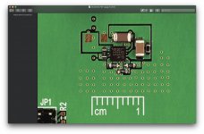
Here is what a regulator circuit looks like for the LT3045. Note the 1cm scale to see that it would fit within a 10mm × 6mm PCB, leaving a bit less than 6mm for the headers connecting the regulator board to the DAC board.
The 22μF CIN capacitor is not shown on the picture, but it could be mounted to the left of the regulator IC, therefore making the board 12mm to 13 wide. This should not be a problem though, because these regulator boards could be mounted parallel to each other on the DAC board.
Attachments
Last edited:
Regulator Board Connectivity
In order to improve the connectivity between the DAC board and the regulator board, we could use 853 and 852 connectors with 6 pins each instead of 3. This would doubles the number of pins per circuit (Input, Output, Ground) and make the connection more mechanically robust. The footprint would be 0.185" × 0.13" (4.7mm × 3.3mm), which translates into 15.51mm². Comparatively, the 12mm × 6mm regulator board would have a surface area of 72mm², 4.6 times larger than the connector's footprint. Modularity and small footprint are two of the main benefits of this approach.
In order to improve the connectivity between the DAC board and the regulator board, we could use 853 and 852 connectors with 6 pins each instead of 3. This would doubles the number of pins per circuit (Input, Output, Ground) and make the connection more mechanically robust. The footprint would be 0.185" × 0.13" (4.7mm × 3.3mm), which translates into 15.51mm². Comparatively, the 12mm × 6mm regulator board would have a surface area of 72mm², 4.6 times larger than the connector's footprint. Modularity and small footprint are two of the main benefits of this approach.
If you used an external clock divider, it would be used along with 45/49MHz clocks to divide the clock frequency in half for all AK4499 playback modes except for up around 768kHz.
The bad part in all this is that anything you between the clock and the dac chip will add jitter.
The additive jitter of a single flip-flop powered by a clean supply is negligible. The clock already has a similar logic buffer at its output. Dividers reduce phase noise by 20log(N) also for an ideal divider. If you care this much about jitter you probably shouldn’t use the higher frequency clocks because they will measure worse than the 22/24.
Last edited:
The additive jitter of a single flip-flop powered by a clean supply is negligible. The clock already has a similar logic buffer at its output.
Agree. I had never observed increasing of jitter, putting 74LVC1G125/04 or similar after oscillator. Influence of the voltage regulator and bypass capacitors is much higher.
Dividers reduce phase noise by 20log(N) also for an ideal divider. If you care this much about jitter you probably shouldn’t use the higher frequency clocks because they will measure worse than the 22/24.
I reality, the jitter is the same with 45/49 + divider" and 22/24 oscillators.
One family oscillators, of course.
Here is what a regulator circuit looks like for the LT3045.
If using that part, maybe better to use the low noise filter cap option at the programming input, and also enable fast startup mode.
If using that part, maybe better to use the low noise filter cap option at the programming input, and also enable fast startup mode.
I understand the fast start-up mode, but I can't find the "low noise filter cap option at the programming input" that you are referring to. Can you point me to a specific page on the datasheet? Thanks!
In order to improve the connectivity between the DAC board and the regulator board, we could use 853 and 852 connectors with 6 pins each instead of 3. This would doubles the number of pins per circuit (Input, Output, Ground) and make the connection more mechanically robust. The footprint would be 0.185" × 0.13" (4.7mm × 3.3mm), which translates into 15.51mm². Comparatively, the 12mm × 6mm regulator board would have a surface area of 72mm², 4.6 times larger than the connector's footprint. Modularity and small footprint are two of the main benefits of this approach.
These connectors are really expensive (about $14 for a plug+socket set) and we'll need 12 per DAC board, but I cannot find any suitable alternative. I'll keep looking though.
Set Pin (Bypass) Capacitance (aka Cset) - Page 19
Noise Spectral Density graph - Page 10
Fast Start Up - Page 19
For ultralow noise applications that require low 1/f noise
(i.e. at frequencies below 100Hz), a larger value SET pin
capacitor is required, up to 22µF.
Protection Features - Page 23
Moreover, to limit
the transient current flowing through these clamps during
a transient fault condition, limit the maximum value of the
SET pin capacitor (CSET) to 22µF.
You read datasheets of devices you are considering? If not, a designer needs to get in the habit it doing that. No time to start like the present. If you have questions about what datasheets say, please ask.
Wasn't trying to make it hard by using the word 'programming', just the way I talk sometimes. Sorry for any confusion.
Last edited:
Set Pin (Bypass) Capacitance (aka Cset) - Page 19
Noise Spectral Density graph - Page 10
Fast Start Up - Page 19
For ultralow noise applications that require low 1/f noise
(i.e. at frequencies below 100Hz), a larger value SET pin
capacitor is required, up to 22µF.
Protection Features - Page 23
Moreover, to limit
the transient current flowing through these clamps during
a transient fault condition, limit the maximum value of the
SET pin capacitor (CSET) to 22µF.
You read datasheets of devices you are considering? If not, a designer needs to get in the habit it doing that. No time to start like the present. If you have questions about what datasheets say, please ask.
Wasn't trying to make it hard by using the word 'programming', just the way I talk sometimes. Sorry for any confusion.
Thanks, this helps a lot.
Yes, I read the datasheets of course, but you have to realize that for a newbie like me, and for complex datasheets like this one, I only get about 10% at first read. A second read will take me to about 20%, and after three or four reads and some early design attempts using the component, I might understand about half of what it's covering. The other half might only come after years of practice I'm afraid. In the meantime, I have to ask for help...
Hopefully, you won't have to repeat yourself too many times though... 😉
Set Pin (Bypass) Capacitance (aka Cset) - Page 19
Noise Spectral Density graph - Page 10
Fast Start Up - Page 19
For ultralow noise applications that require low 1/f noise
(i.e. at frequencies below 100Hz), a larger value SET pin
capacitor is required, up to 22µF.
Protection Features - Page 23
Moreover, to limit
the transient current flowing through these clamps during
a transient fault condition, limit the maximum value of the
SET pin capacitor (CSET) to 22µF.
You read datasheets of devices you are considering? If not, a designer needs to get in the habit it doing that. No time to start like the present. If you have questions about what datasheets say, please ask.
Wasn't trying to make it hard by using the word 'programming', just the way I talk sometimes. Sorry for any confusion.
Reading your comments and the datasheet, I guess we should use a 22µF capacitor on CSET. LDOVR uses the T495C226K025ATE300 tantalum capacitor for CIN. Is it fair to assume that the same capacitor could be used for CSET as well?
The input cap should be ceramic or tantalum || ceramic. The SET pin cap could go either way. I would probably choose a ceramic cap there because I don't have much concern about piezoelectric effects in a stationary desktop device, but it is a concern at that node in general. The tantalum would be ok, but since the goal of the large cap is to lower LF noise, I wonder about the LF noise of tantalum and aluminum electrolytic caps here. I haven't found a ton of info or measurements except that it tends to follow DC leakage, so a 22 uF hybrid polymer Al electrolytic might be better than a tantalum. An interesting option, that I have never tried or tested, is an acrylic capacitor like the Rubycon PMLCAP. A bit large and limited to 16V, but it looks cool anyway:
16MU226MD35750 Rubycon | Capacitors | DigiKey
16MU226MD35750 Rubycon | Capacitors | DigiKey
Last edited:
The input cap should be ceramic or tantalum || ceramic. The SET pin cap could go either way. I would probably choose a ceramic cap there because I don't have much concern about piezoelectric effects in a stationary desktop device, but it is a concern at that node in general. The tantalum would be ok, but since the goal of the large cap is to lower LF noise, I wonder about the LF noise of tantalum and aluminum electrolytic caps here. I haven't found a ton of info or measurements except that it tends to follow DC leakage, so a 22 uF hybrid polymer Al electrolytic might be better than a tantalum. An interesting option, that I have never tried or tested, is an acrylic capacitor like the Rubycon PMLCAP. A bit large and limited to 16V, but it looks cool anyway:
16MU226MD35750 Rubycon | Capacitors | DigiKey
It looks really cool indeed. It's also quite expensive... Would you consider it for CIN, CSET, or both?
Question about clocks
Looking at the latest PCB layout, I am trying to figure out the best way to fit all the components that are needed by the two clocks. If we consider the AMB o1 as reference point (thank you Mark!), it's clear that we have to fit quite a bit, and if we try to put all that directly on the DAC board, it is quite unlikely that we could get the clocks' outputs close to the DAC chip's MCLK pin.
An alternative approach would be to mount all this on a separate clock board that would be connected to the DAC board through a header for power and clock selection and an SMP coaxial board-to-board connector for the clock signal (Cf. page 22 of this brochure, thank you again Mark). If we were to do so, we could mount the SMP connector as close as we want to the MCLK pin on the DAC board and as close as we want to the clocks' output resistors on the clock board.
It would also make it much easier to pick good crystals from a batch, because most of the BOM costs for this clock board would come from the crystals. Therefore, we could fabricate a whole bunch of boards, test them on a DAC directly, and only keep the ones that work well. And it would make it easier to test different crystals. Furthermore, it is quite likely that we could mount an LT3042 regulator board flat on the clock board, thereby making this subsystem modular as well, which would further reduce the BOM cost of the clock board itself.
Would that be an acceptable option?
Last edited:
It looks really cool indeed. It's also quite expensive... Would you consider it for CIN, CSET, or both?
Only CSET, which is the reference filter. The datasheet mentions the effect is negligible for input and output caps due to the PSRR and low output Z. I probably would just use a 22uF X7R myself. Another option that may be better than the tantalum (but larger) is the Al hybrid like I mentioned before:
EEH-ZC1V220R Panasonic Electronic Components | Capacitors | DigiKey
Actually, that particular tantalum they used probably has around the same leakage, but higher ESR. Since it's not a polymer tantalum, keep in mind it has to be derated by 50%.
Last edited:
- Home
- Source & Line
- Digital Line Level
- 8 × AK5578EN + 8 × AK4499EQ ADC/DAC Boards