Presumably, they wanted to keep the impedance of the caps very low as seen by the dac chip. Traces have resistance, as do connectors. If caps are rated with ESR of milliohms, how much more resistance are you sure is safe to add and and still benefit from full performance. Also, the longer wires run to caps, the bigger the current loops are. How will you maintain minimal series resistance, and how will you maintain minimal current loop area to avoid noise pickup and other stray coupling?
Makes sense.
I probably wouldn’t put the caps on another board. You have a lot on separate boards as it is. I’d probably prototype this in a less modular way but with larger than final form-factor if you really feel the need to test all these options.
Got it!
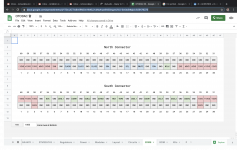
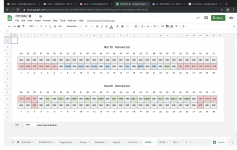
OTODAC™ Spreadsheet
I've moved all the sheets related to the DAC onto a separate OTODAC™ spreadsheet. This will make it easier to follow this particular project.
I've moved all the sheets related to the DAC onto a separate OTODAC™ spreadsheet. This will make it easier to follow this particular project.
Redesigned OTOBUS™
Following the advice of a reader, I have redesigned the OTOBUS™ in order to provide more ground return circuits for the parts of the bus that matter most: the I²S and SAI interface. There, every single circuit is just a pin away from a ground return pin, and sometimes to adjacent pins are available for ground returns.
This came at a cost though: all the power supply lines at the exception of 5V had to go. This design was motivated by the fact that most bricks will be perfectly happy with 5V, and the ones that are not (DAC and ADC bricks for example) will need very specific power levels. Therefore, there really wasn't much sense trying to back that into the core OTOBUS™ architecture.
Instead, we're much better off leaving that to the brick, simply providing enough current through multiple 5V lines. As a result, the OTOBUS™ has two 5V line, and knowing that every brick comes with two OTOBUS™ connectors, this gives us 4 lines in total for every brick. And knowing that the ERF8/ERM8 connectors used for the OTOBUS™ are rated at 2.2A per pin with 2 pins powered, that gives us a theoretical total of 8.8A per brick. Furthermore, the DAC brick is a 3 OTO™ unit brick, therefore could get a theoretical total of 26.4A. Clearly, we will never get anywhere close to that...
How about one +8v line? I will be willing to lose one of four 5v lines.
We have to work at the level of a single OTO™ connector, which means that we would have to trade one of the two 5V lines for an 8V line (see updated sheet). I am willing to consider doing that, but I need to justify the 8V level. Why did you pick that value instead of 6V or 10V or any other value? What makes is the most natural choice?
We have to work at the level of a single OTO™ connector, which means that we would have to trade one of the two 5V lines for an 8V line (see updated sheet). I am willing to consider doing that, but I need to justify the 8V level. Why did you pick that value instead of 6V or 10V or any other value? What makes is the most natural choice?
IME, it is high enough to provide improved regulation performance from ADM7150, but not so high as to cause unnecessary heating and power dissipation in the regulator. 7v might be good enough, still better than 5v, IME. Its also high enough to allow for local regulation of 5v if needed. However, your project to do with as you wish.
IME, it is high enough to provide improved regulation performance from ADM7150, but not so high as to cause unnecessary heating and power dissipation in the regulator. 7v might be good enough, still better than 5v, IME. Its also high enough to allow for local regulation of 5v if needed. However, your project to do with as you wish.
Got it!
For this power supply, I feel like there is no right answer. For my applications, I will use USB, therefore I'll stick to 5V. For your application, you might want to use the OTO™ connector to connect to the MCU, but you will probably provide this 8V directly, not from the 5V coming out of the USB port. And other applications might still need something else. Therefore, I suggest that the "standard" OTO™ sticks to 5V for both power pins (1 and 20, Cf. sheet), but that we designate pin 20 as "XV", "X" being application-dependent (you pick what you want for your application). This would not make your module compatible with other modules that use a different voltage, but that's the price to pay for this level of modularity.
Connectors for DAC Board
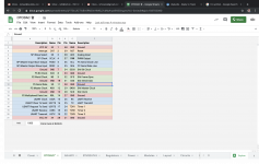
I have done a detailed analysis of the logic and signal pins that we need to handle on the AK4499. Nine of them can be hardwired. The others will need to be driven by the MCU. This allowed me to create this list of circuits that need to be handled by the connectors going from the DAC board to the interface board, which will play a dual role: interface to the MCU board (what is called the "Plate Board") and first-stage power regulation (feeding from the USB's 5V). On the power side, the set of required circuits was driven from this power supply design.
Taking all that into consideration and looking at the pinout for the AK4499 DAC chip, I designed the pinouts for the two ERM8 connectors that will connect the DAC board to the interface board. And because we need much less pins that originally thought, I got rid of the two UMPT connectors, and I made sure to provide as many ground return circuits as possible.
I dedicated three pins for clock selection. One will be used to select the clock frequency, another to select clock division, and the third to by-pass the built-in clock and feed from an external clock. The MCLK pin on the North connector will feed whichever clock is selected back to the interface board.
Most power circuits have been doubled in order to spread their loads and get some level of redundancy. Knowing that we have so many pins dedicated to ground returns, I wonder if some of them could be used to double some logic and signal pins as well. I assume that doing so for digital signal circuits could induce some unwanted jitter, but I'd love to get some confirmation on that.
Attachments
Last edited:
For this power supply, I feel like there is no right answer. For my applications, I will use USB, therefore I'll stick to 5V.
The dac chip needs regulated 5v, 3.3v and 1.8v. Those are aside from the regulated voltages needed for each channel. How are you planning to regulate the +5v?
Last edited:
The dac chip needs regulated 5v, 3.3v and 1.8v. Those are aside from the regulated voltages needed for each channel. How are you planning to regulate the +5v?
As Chris said, we'll boost it to 6V or 6.5V first, then bring it down to 5V again.
Remember: our power comes from USB. We do not have anything else.
I would boost to 6.5V.
Why 6.5V? If you want 5V in the end, can't we do 5.5V or 6V? Any reason to go higher?
And same question for 3.3V and 1.8V. We'll want to get these from slightly higher levels, so what should these levels be? Obviously, we want the difference between input and output to be as low as possible in order to minimize dissipation and we can't have the delta lower than what the LDO is capable of handling, but is there a reason to have a delta significantly higher than the minimum supported by the LDO?
Yes, there is a reason for going higher. LDO regulation is better with a higher delta, but there is a limit to that. That's true for other linear regulators as well.
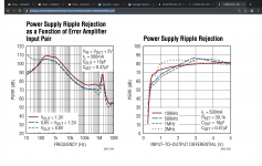
IME (in my experience), using ADM7150 to produce 3.3v with 5v input resulted in less than optimal regulation. IMHO, 7v was sufficient. I only suggest 8v to allow some tolerance. For ADM7150, the data sheet page 11 shows PSRR (power supply rejection ratio) vs input headroom, but PSRR may not be the whole story. I could hear a difference using ADM7150 for 3.3v AVCC as input voltage was adjusted, and distortion from the regulator didn't seem to level out until about 7v input. That amounts to 3.7v of headroom. Above 7v I could not hear any further improvement. In the event anyone claims I am imagining things, I still have the regulators and you can test them for AVCC yourself. You may also want to consider the implications if 5v output were to be needed.
Last edited:
Yes, there is a reason for going higher. LDO regulation is better with a higher delta, but there is a limit to that. That's true for other linear regulators as well.
IME (in my experience), using ADM7150 to produce 3.3v with 5v input resulted in less than optimal regulation. IMHO, 7v was sufficient. I only suggest 8v to allow some tolerance. For ADM7150, the data sheet page 11 shows PSRR (power supply rejection ratio) vs input headroom, but PSRR may not be the whole story. I could hear a difference using ADM7150 for 3.3v AVCC as input voltage was adjusted, and distortion from the regulator didn't seem to level out until about 7v input. That amounts to 3.7v of headroom. Above 7v I could not hear any further improvement. In the event anyone claims I am imagining things, I still have the regulators and you can test them for AVCC yourself. You may also want to consider the implications if 5v output were to be needed.
Got it!
The LT3045 datasheet does not have as many charts for PSRR analysis. These two charts on page 10 suggest that 2V might be a sweet spot (high enough to provide good performance, but low enough to keep dissipation as low as possible).
I've updated the power scheme, circuits, and connectors accordingly.
Thanks!
Attachments
Last edited:
Updated Power Supply Architecture
Just to clarify, based on the previous discussions, I think we can simplify our PSU board and only use 3 × LTM8045 and 2 × LTM8049:
- 1 × LTM8045 to boost 5V to 7V for analog components
- 1 × LTM8045 to boost 5V to 7V for digital components
- 1 × LTM8045 to boost 5V to 17V
- 2 × LTM8045 to boost 5V to ±17V
From there, the PSU board would provide the following supplies (Cf. Circuits):
- 5V
- A7V
- D7V
- 17V
- +17V
- -17V
And here is what the new connector pinouts would look like.
Since everything gets regulated again on the DAC board, I'm not sure that we need separate first-stage regulators for 7V though, and maybe we can save one LTM8045. Any strong opinions on the matter?
Attachments
Last edited:
Improved OTOBUS™
This might be an insignificant change, but I've moved things around on the OTOBUS™ in order to get the critical I²S and SAI interfaces in the center of the connector, away from the power supply lines, which are located on the edges.
This might be an insignificant change, but I've moved things around on the OTOBUS™ in order to get the critical I²S and SAI interfaces in the center of the connector, away from the power supply lines, which are located on the edges.
Attachments
Presumably, they wanted to keep the impedance of the caps very low as seen by the dac chip. Traces have resistance, as do connectors. If caps are rated with ESR of milliohms, how much more resistance are you sure is safe to add and and still benefit from full performance. Also, the longer wires run to caps, the bigger the current loops are. How will you maintain minimal series resistance, and how will you maintain minimal current loop area to avoid noise pickup and other stray coupling?
I kept thinking about this and looked for the resistance of connectors like Mil-Max machined carrier sockets. They're in the range of 10mΩ. The ESR of 16SVPK1200M is 12mΩ. And the ESR of EEHZK1E561UP is 20mΩ. Therefore, I am very tempted to solder 4 × EEHZK1E561UP directly on the DAC board and provide sockets for another four capacitors, which could be the 16SVPK1200M or anything else we want. The mating height of the carrier sockets is 2.2mm, which means that mounting capacitors on a 0.8mm thick PCB would only raise them by 3mm.
Chris, I know that you recommended against an extra mezzanine board, but going with this hybrid approach (one soldered and one on a mezzanine, Cf. layout) might create an interesting tradeoff (I really, really like the idea of making it easy to try different capacitors on the final form factor).
Receptacles with OFP Solder Barrier
These Mil-Max 4015 Receptacles with OFP Solder Barrier look awesome. This application note does a great job of explaining how they work. Using these would allow us to reduce the lengths of connections to mezzanine boards and vertically-mounted regulator boards, thereby reducing EMI and increasing the permitted height of our regulator boards. I am now looking at the best mating pins for these.
These Mil-Max 4015 Receptacles with OFP Solder Barrier look awesome. This application note does a great job of explaining how they work. Using these would allow us to reduce the lengths of connections to mezzanine boards and vertically-mounted regulator boards, thereby reducing EMI and increasing the permitted height of our regulator boards. I am now looking at the best mating pins for these.
These Mil-Max 4015 Receptacles with OFP Solder Barrier look awesome. This application note does a great job of explaining how they work. Using these would allow us to reduce the lengths of connections to mezzanine boards and vertically-mounted regulator boards, thereby reducing EMI and increasing the permitted height of our regulator boards. I am now looking at the best mating pins for these.
And this edge-mount pin is a perfect match. The application note shows how it works. In combination with the receptacle linked above, these would be perfect for the regulator boards.
- Home
- Source & Line
- Digital Line Level
- 8 × AK5578EN + 8 × AK4499EQ ADC/DAC Boards