I put the 100nF in parallel with a 220uF in that sim as I often see a ceramic bypass across the electrolytic.
Is 220uF too high for that application, or doesn't matter so much?
Is 220uF too high for that application, or doesn't matter so much?
I think here a good quality 1uF unpolarized cap is enough...the amplifier is already silent, the main goal of this mod idea is to cut the remaining 50 or 100hz noise comming from the power supply...that capacitor is for filtering noise, not for audio band-pass. There's nothing below 50Hz, even in a SMPS...
I dont't play with simulator, but a friend of mine did and with a 100uF cap and 100mV-PP injected in the power supply, the resistors also 100k and 82k the noise rejection increased from -57 to -75dB...
But mixing this result with the theory I know, keeping account of the high value of the resistors, I think 1uF or, let's admit 10uF good electrolytic could do the job, without modifying the existing PCB. just pull out the 180k resistor, put two 100k+82k series and from the midpoint you can tie a capacitor, the other end to GND.
I put the 100nF in parallel with a 220uF in that sim as I often see a ceramic bypass across the electrolytic.
Is 220uF too high for that application, or doesn't matter so much?
Ooops!. I misread your 220uF as 220pF.
Yes 220uf is more than enough. Probably too much as the long time constant with the resistor to the power rail means the bias voltage comes up rather slowly at switch on. I would think 22uF would be plenty and by all means add a small film cap in parallel.
Cheers
Ian
Some quick results
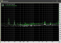
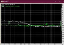
I made the changes to the power supply to the driver transistors as previously detailed:
Remove 180K and replaced with 82K and 100K in series
Connected mid point to 22uF and 100nF to ground
Measured using the power supply labelled 'XP' and 'Boost' (phone charger- > Boost Converter)
Same configuration as before:
Power supply -> CRC -> LM317 -> VCC
All with a 245ohm load @ -3dB.
Here is the comparison with before:
XP:

Boost:

As you can see, the noise floor was worse using 'XP', but the boost converter faired much better and is now quiet with no input connected.
There was a change to the enclosure in that a layer of aluminium was applied to the inside surfaces to assist with shielding (plastic case), so that might be a factor in these tests, and something that I'll look into more when I get a chance.
I made the changes to the power supply to the driver transistors as previously detailed:
Remove 180K and replaced with 82K and 100K in series
Connected mid point to 22uF and 100nF to ground
Measured using the power supply labelled 'XP' and 'Boost' (phone charger- > Boost Converter)
Same configuration as before:
Power supply -> CRC -> LM317 -> VCC
All with a 245ohm load @ -3dB.
Here is the comparison with before:
XP:
Boost:
As you can see, the noise floor was worse using 'XP', but the boost converter faired much better and is now quiet with no input connected.
There was a change to the enclosure in that a layer of aluminium was applied to the inside surfaces to assist with shielding (plastic case), so that might be a factor in these tests, and something that I'll look into more when I get a chance.
Attachments

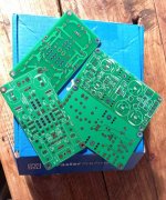
After I receive the PCBs from knauf1919, I will prepare some kits with this set of PCB, if anyone interested, send me a message. 2-3 sets will be available, PCB+components or PCB mounted and tested. I will come back with assembled ones photos. The set of PCB contains one PCB for the amplifier and one for the denoiser/stabilised power supply.
Last edited:
Sorry, you can clarify what kind of resistors we are talking about. Scheme from which post - Prasi’s layout from post #152 or from the very first post of the topic?If you would make R1&R6=18Ohm and R8=12Ohm bias current would be ~ doubled at 170mA.
Thanks.
Victor
Refering to the post #1 schematic.clarify what kind of resistors we are talking about
Thanks. Wouldn't lowering the resistance for the input transistor (U1) be dangerous? To what extent will this be acceptable?
Hello, this is my version headphone amplifier based on lineup circuit. Made for portable purpose, the circuit is supplied by 3.7V x 2 (7.4V)


With load 47 Ohm, the output voltage is 3.78Vpp and output Impedance is 1.4 Ohm
With load 47 Ohm, the output voltage is 3.78Vpp and output Impedance is 1.4 Ohm
Last edited:
I'm curious how R1 and R6 behave, how hot they are? In conditions where the supply voltage is lower.
Super fine work. A job well done.
Super fine work. A job well done.
You will have to watch power dissipation of the parts.Thanks. Wouldn't lowering the resistance for the input transistor (U1) be dangerous? To what extent will this be acceptable?
At 12V and ~165mA current this will be ~0.6W for Q1, ~0.5W for R1&R6 each and ~0.35W for R8. You´ll definitely need a heatsink for Q1 and size the resistors accordingly.
If you don´t have headphones <32Ohm you probably don´t need that much bias though.
Nice job! Gotta love compact layouts and SMD.Hello, this is my version headphone amplifier based on lineup circuit.
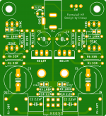
Hello all,
first of all thanks to Lineup for the design..
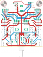
made a layout has dc and signal input and hp out jacks are on the board, measures 53x58 mm..
BD140s will be sandwiched between case and underside of the board so has screw holes..
since i'm not expert for pcb design, there may be something wrong..
can someone with sharp eyes take a look please?
thanks in advance.
first of all thanks to Lineup for the design..
made a layout has dc and signal input and hp out jacks are on the board, measures 53x58 mm..
BD140s will be sandwiched between case and underside of the board so has screw holes..
since i'm not expert for pcb design, there may be something wrong..
can someone with sharp eyes take a look please?
thanks in advance.
Attachments
Last edited:
why did you use BD140?
the final transistor must be NPN, ie BD139.
C3 is backwards
marin cornel, avtech thanks a lot. C3 rotated.
bd140 from another pcb, exactly on same place..
forgot the change label..
Attachments

Lots of your parts are pretty close with some even overlapping.
(C5/R9; C2 seems pretty much "sandwiched"; 560C/C3).
Just make sure these will fit in reality.
R3 is on the bottom? and uses the same through-holes as PJ307 and C2?
(C5/R9; C2 seems pretty much "sandwiched"; 560C/C3).
Just make sure these will fit in reality.
R3 is on the bottom? and uses the same through-holes as PJ307 and C2?
joensd, thank you very much.
actually this is just a quick layout to see if there is a mistake and
will be fine tuning for parts placements.
yes, R3 is on the bootom side, sharing footprints of C2 and PJ307.
actually this is just a quick layout to see if there is a mistake and
will be fine tuning for parts placements.
yes, R3 is on the bootom side, sharing footprints of C2 and PJ307.
Attachments

- Home
- Amplifiers
- Headphone Systems
- 3 Transistor HP Amplifier with low dist