This is a response to a previously deleted (or censored?) message:
Let's see, what Santa drops ...
Note: It is not a MUST to present pictures of build SA2016 amplifier modules.
IMHO: Most important is that AndrewT enjoys the sound of the result and others now know, that this amplifier is verified to work if you build it correctly.
BR, Toni
Let's see, what Santa drops ...
Note: It is not a MUST to present pictures of build SA2016 amplifier modules.
IMHO: Most important is that AndrewT enjoys the sound of the result and others now know, that this amplifier is verified to work if you build it correctly.
BR, Toni
Have a look at the url: https://www.schaeffer-ag.de/en
Unfortunately the price is rather high ...
Modu did a good job with my heat spreaders - perhaps cheaper? YMMV 😉
Happy New Year everyone!
As followers of this thread know, I am building Toni's SA2013/4 200W 8R amp, the amplifier for which this thread was originally started. Toni has been extremely helpful answering all my (far too many!) build questions. It has been my first amp build.
I have some questions as I try to understand the circuit better and since many of these are newbie questions I thought I would ask them here because (a) others may be able to share the load of answering them and (b) others may also be interested in the answers. I have bolded questions below to highlight them from my rambling.
I think I understand the input stage. Please correct any poor terminology or misunderstanding on my part in the following. There is a cascoded input differential pair with emitter degeneration, a current source implemented by Q2 (and ancillary parts) and a current mirror in the form of Q1, Q8 and Q5 although I have not seen a current mirror in this form. Does it have a name? Given it seems to have evolved from the simple current mirror in post 1 I should try to see if it was discussed in this thread.
I "get" the three compensation methodologies provided for.
Q11 provides a current source for the bias spreader.
I'm struggling with the single-ended VAS. Which components are protection features rather than core to the VAS operation? I recognise the post 1 VAS as a Darlington but don't understand the function of that circuit's Q8. The VAS in the final schematic has evolved from the first... 😱
Lastly for the IPS/VAS, the feedback network resistor has been split into two - 18k || 15k. For power dissipation reasons? (I see that 18k || 15k = 8.2k and so matches R5.) Doesn't using two parallel greater resistances lead to greater noise?
On the OPS, obviously the output transistors are paralleled for SOA purposes. Am I right to see the OPS as having just a single driver stage, with the drivers Q33 and Q35 (and Q34 and Q36) paralleled for SOA and current limiting implemented via Q32 and Q31 plus associated resistors?
Thanks for any help!
I changed the two paralleled NFB resistors which have a high voltage across them when high output transients occur.
I cut the trace where they mount to allow the two SMD resistor to operate in series, thus halving the voltage peak. ( I did the same for the other two paralleled resistors in the collector of the EF helper transistor.
I used 4k02 & 4k32 which I happened to have in stock in thin film. smd 805 fits quite nicely across the close spaced through hole pads. And it's the total resistance that determines the Johnson noise.
The component numbers in my ver 14 don't agree with your post's numbering, so I'll hold off answering the questions with part numbers.
Last edited:
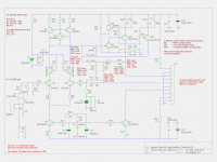
Sorry I meant to repost Toni's schematics so it was clear what I was referring to. I was interrupted and then timed out. See attached reproduced from post 1145.
Ah ok so when paralleled the Johnson noise is 'paralleled' also. Thx.
And it's the total resistance that determines the Johnson noise.
Ah ok so when paralleled the Johnson noise is 'paralleled' also. Thx.
Attachments
Last edited:
The 8pairs of output BJTs draw a large base current.
the drivers need to be beefed up to meet that demand.
The three transistors are still a current mirror.
https://en.wikipedia.org/wiki/Current_mirror
At the bottom there are links to Widlar and Wilson versions.
Read all three and how they operate and what needs to be matched.
the drivers need to be beefed up to meet that demand.
The three transistors are still a current mirror.
https://en.wikipedia.org/wiki/Current_mirror
At the bottom there are links to Widlar and Wilson versions.
Read all three and how they operate and what needs to be matched.
Hi Andrew. Yes, I understand the paralleling of the drivers to meet the needs of the paralleled output transistors. I was wanting to confirm my understanding of the typology as described above.
I also understand that the three transistors are a current mirror. I have just not seen this sort of mirror before. It's not a Wilson obviously.
I also understand that the three transistors are a current mirror. I have just not seen this sort of mirror before. It's not a Wilson obviously.
D. Self discusses this in his book APAD6 page 133-134. As he couldn't find a name for this type of current mirror (with added base current compensation) he called it EFA current mirror ("emitter follower added"). This type of current mirror has a higher accuracy as the standard current mirror and using tranistors with higher beta it has nearly the same performance as the wilson current mirror.There is a cascoded input differential pair with emitter degeneration, a current source implemented by Q2 (and ancillary parts) and a current mirror in the form of Q1, Q8 and Q5 although I have not seen a current mirror in this form. Does it have a name? Given it seems to have evolved from the simple current mirror in post 1 I should try to see if it was discussed in this thread.
Q10 and ZD2 are for protection only. Current limiter for the VAS.I'm struggling with the single-ended VAS. Which components are protection features rather than core to the VAS operation?
Yes. This is also part of the name of the amplifier "2stage ef"On the OPS, obviously the output transistors are paralleled for SOA purposes. Am I right to see the OPS as having just a single driver stage, with the drivers Q33 and Q35 (and Q34 and Q36) paralleled for SOA and current limiting implemented via Q32 and Q31 plus associated resistors?
The driver and ops transistors together do have a high beta so I decided to not use a 3 stage EF ops design.
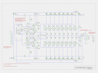
(part numbers in reference to schematics from post #1865)
BR, Toni
Thanks again Toni. I will spend some more time with it.
BTW I am LOVING the performance of this amp. It received another very thorough workout today and I continue to be very impressed. My Krell FPB-200 is about to go back in its box!
BTW I am LOVING the performance of this amp. It received another very thorough workout today and I continue to be very impressed. My Krell FPB-200 is about to go back in its box!
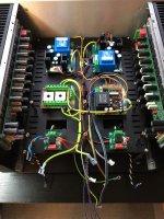
One surprising thing I encountered with this build was in respect of the 2mm iron shelf. In the image attached you can see a shelf holding the Aux Supplies (1 per channel), Main Controller Unit (housekeeping), Star Ground and Output Relays. I had this shelf made in 2mm iron (anodised) with a view that it would help shield (Faraday cage) the OPS (and IPS/VAS which sit on another shelf attached to this one) etc from the main power supplies below.
Interestingly I found that the PCB transformers in the two auxiliary supplies and the MCU radiated interference into the iron shelf and it was being picked up everywhere. I could literally connect my sound card to the iron shelf and watch in ARTA Spectrum Analyser and see this interference as each of these PCB transformers powered up. Interference from the main PSUs was considerably less, presumably because the main toroids are well-shielded and they sit below the shelf. I mocked up a shelf in cardboard and found I got lower noise at the output of the amp.
As an initial step to try to improve the situation I had the shelf redone in aluminium. I also made some improvements to the GND wiring as advised by Toni. Lastly I purchased some 12.7mm soft iron box section from metals4u.co.uk, cut it length and spray painted it, added end caps for aesthetics and then routed the output of the OPS to the output relay boards via this tubing. See pic attached.
The next idea is to consolidate the three ancillary PSUs (2 x Aux and 1 x MCU) into one. With a low leakage transformer, staying under 1W when the amp is in standby should be achievable as Toni's MCU uses very little current when in this state. I've made a largely SMD version of Toni's MCU (the PCB is 85x35mm). +/-12V is supplied to it from a single PSU of the builder's choice and with some minor logic alterations to the software provided by Toni it controls the onward supply of power to inrush relays, output relays and auxiliary devices (such as balanced to single-ended input boards in my case) when the amp is turned on. More on this later...
Attachments
Last edited:
...
Interestingly I found that the PCB transformers in the two auxiliary supplies and the MCU radiated interference into the iron shelf and it was being picked up everywhere.
...
Iron tube is grounded at least near output sockets?
I know it is hard to get the output noise down to the test bench measured level of -127dB (A-w) if all components are mounted in a case.
Really amazing build!
BTW: I'm loving the sound too! Absolutely pure sound energy!
BR, Toni
Good point. At the moment, no. And there is no metal-metal contact between the iron tubing and the aluminium shelf as the two are affixed with strong, padded, double-sided tape. I will have to find a way to connect a drain wire to the tubing and attach it to the aluminium shelf.
PS: I might have to do another mono block for my centre channel so that all of my front sound stage is driven by the same amp...😱
PS: I might have to do another mono block for my centre channel so that all of my front sound stage is driven by the same amp...😱
...
PS: I might have to do another mono block for my centre channel so that all of my front sound stage is driven by the same amp...😱
You could build a SA2015 V-MOSFET or an SA2016 L-MOSFET amplifier. These amplifiers have enough power to drive your center speaker and have the same gain as the big SA2014 😉
Depending on the used transistor types and power supply they can deliver up to 120W@8R.
BR, Toni
Last edited:
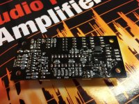
I've made a largely SMD version of Toni's MCU (the PCB is 85x35mm).
A couple of quick 'n dirty pics of the as yet untested SMD MCU board...
Attachments

Is it a protection board?A couple of quick 'n dirty pics of the as yet untested SMD MCU board...
Is it a protection board?
Dear Thimios,
it is more or less the shrinked variant without power supply of this housekeeping circuit:
housekeeping controller V4.x
You still need the speaker output relay boards and inrush current control board (115/230V relay board).
The MCU controls power on toroid inrush current, DC on speaker outputs, 5 x overtemperature, external power on (with configurable chain delay). Controlled delay after subsequent power on requests to be child safe.
BR, Toni
Indeed.
The action of the output relay control is changed a little and requires a modest change on the output relay board from before. In Toni's earlier circuit the MCU controlled a transistor on the output relay board on the low side of the relay to allow current to flow through it while the output relay was supplied 12V from some other PSU (the mains supply to which was controlled by one of the relays on the in-rush board). With this version, 12V (and -12V) is supplied to the MCU the MCU controls the onward supply to the output relay. So the output board can be simplified a little. (The extra relay on the in-rush board will become redundant in my setup.)
The added feature is the MCU can switch the supply of -12V/+12V via two 4 pin connector headers.
Attachments
Last edited:
Yes i see,just a different MCU board.
I'm looking for a simpler (cheaper)version. of protection.🙁
There isn't money any more in Greece.🙁🙁🙁
I'm looking for a simpler (cheaper)version. of protection.🙁
There isn't money any more in Greece.🙁🙁🙁
Last edited:
- Home
- Amplifiers
- Solid State
- 2stageEF high performance class AB power amp / 200W8R / 400W4R