Me, more or less.
The capacitance is intended to simulate the effect of speaker cable capacitance and speaker stray capacitance, especially from transformers in electrostatic models.
These all attach after the output inductor, it's precisely the point of the inductor, to isolate these loads.
So that's the traditional test.
But it doesn't seem like a bad idea to check the sensitivity of the amp to stray layout capacitance as well. Hence before the inductor.
But realistic values at this point will tens or maybe a few hundred pF.
Best wishes
David
When I simulate my amps I do simulation with the cap connected before inductor, and with the cap connected after inductor, example here.
http://www.diyaudio.com/forums/solid-state/243481-200w-mosfet-cfa-amp-14.html#post3668842
PS. we had similar discussion that time.
Last edited:
When I simulate my amps I do simulation with the cap connected before inductor, and with the cap connected after inductor, example here.
http://www.diyaudio.com/forums/solid-state/243481-200w-mosfet-cfa-amp-14.html#post3668842
PS. we had similar discussion that time.
Have you retested this with 70nF on the latest release too? Real life test?
BR, Toni
Have you retested this with 70nF on the latest release too? Real life test?
BR, Toni
No, I was afraid to do that.
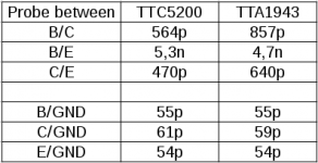
For the 200W brother I've measured about 800pF stray capacitance from output to heatsink (grounded) using 8 pairs of TTC5200/TTA1943 so for simulation I think it is really necessary to add some hundred pF Cload before Zobel/Thiele network. What do you mean?
BR, Toni
Much of that 800pF should be the collector-emitter capacitance of the output devices (hence already included in the simulation). Don’t forget that the collector is connected to ground via the DC bus bypass capacitors. You therefore have Cce in series with the DC bypass caps and it’s (mostly) this that you are measuring. As the bypass caps are very much larger than 800pF, the device parasitic capacitance will dominate.
Of course there is also the stray capacitance via the heatsink, which appears in parallel with (Cce+DC bypass). If you want to get a good idea of what this is, you need to cut some copper tape to the size of the transistors’ collector tab, stick this to the heatsink (with your thermal interface in between) and measure the resulting capacitance with your meter.
Much of that 800pF should be the collector-emitter capacitance of the output devices...
Thanks Harry for that explanation, I suspected some such issue, that's why I asked how it was measured.
It should be possible the disconnect the bypass capacitors and measure directly but I think my calculations of the stray capacitance have not been discredited and still look reasonable.
So for the moment I will still use my calculated values as an approximation, interested to see what Toni's corrected real measurements are.
Best wishes
David
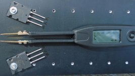
Here some measurements using single mounted BJTs (isolation provided by keratherm red 86/82). Collector of BJT's is internally electrically connected with copper back plane. The copper backplane has a capacitance of about 59p-61p to the heatsink per BJT (TTC5200/TTA1943).
Measurement frequency was 200mV RMS @ 10kHz
Now the (noob = me) question: can the measured 54p between emitter and heatsink/GND completely be ignored as they are measured in series with collector/emitter which is already included in the bjt spice model or is this stray capacitance at least partially effective?
Attachments
...Now the (noob = me) question...
That's not a noob question😉 Actually I think it's a pretty subtle one.
I suspect the capacitance from the output to the heat-sink is screened by the collector metalwork Seems that the metal plate should act as a Faraday shield but it's not obvious to me. Hmm.
Best wishes
David
The power device backplate is electrically the same as the Drain/Collector of the device.
Capacitance between backplate and surroundings is effectively the same as capacitance from Drain/Collector to surroundings.
For a Lateral mosFET where Source is the backplate, it is equivalent to Source to surroundings capacitance.
Capacitance between backplate and surroundings is effectively the same as capacitance from Drain/Collector to surroundings.
For a Lateral mosFET where Source is the backplate, it is equivalent to Source to surroundings capacitance.
Thought about. Think Harry is right. The measured emitter capacitance to the copper plate capacitance is only seen through the bjt's internal capacitance. C/E capacitance is about 10 times bigger as the C/GND capacitance. Real capacitance from emitter to copper would be very low due to the small die size. So the measured capacitance is more or less only another (but small) blocking capacitor from collector to GND.
...For a Lateral mosFET where Source is the backplate...
I didn't know they did that, but I've never used lateral MOSFETs.
Seems like a bad idea for stray capacitance in typical EF OPS.
Best wishes
David
...Real capacitance from emitter to copper would be very low due to the small die size...
So we are all in accord that the effective value is much smaller than you measured?
Best wishes
David
And therefore not much of a problem?
So we are all in accord that the effective value is much smaller than you measured?
Best wishes
David
And therefore not much of a problem?
No problem - only if we would use lateral MOSFETS where source is connected to copper plate. 😀
Stability near clipping
Some findings...
during positive offset:
during negative offset;
This may explain an old real life measurement result in this thread: during cherry compensation tests oscillations where mostly seen at positive halfwave near clipping.
Some findings...
during positive offset:
- as phase margin decreases, gain margin increases
during negative offset;
- as phase margin decreases, gain margin increases
- stability is better during negative halfwave
This may explain an old real life measurement result in this thread: during cherry compensation tests oscillations where mostly seen at positive halfwave near clipping.
Attachments
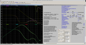

...positive offset...
Looks like you have used my technique, you have any problems, comments or ideas for improvements?
Your results show a bit less loss of PM than mine, perhaps (probably?) because your VMOSFET outputs lose a bit less speed than the BJTs in my simulation.
Always of interest to see how different circuits respond.
Also I use a symmetrical circuit with push-pull VAS so +ve and -ve are similar.
Best wishes
David
Last edited:
Try switching to the improved models for those MOSFETs:
http://www.diyaudio.com/forums/soft...-power-mosfet-models-ltspice.html#post4172517
It might even speed up simulation.
http://www.diyaudio.com/forums/soft...-power-mosfet-models-ltspice.html#post4172517
It might even speed up simulation.
Try switching to the improved models for those MOSFETs:
http://www.diyaudio.com/forums/soft...-power-mosfet-models-ltspice.html#post4172517
It might even speed up simulation.
... for this 50W mosfet amplifier I'm already using the new models from Bob Cordell (I have added the IRFP*Ckst models to the "Cordell-Models.txt" file - see asc and "needed_libs.zip" some posts above) 😉
Thx, Toni
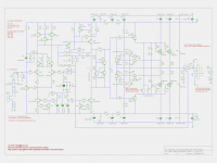
... as the preliminary schematic is nearly finished ...
Hi Toni
By coincidence I have just posted a few comments on Bob's thread about why I don't think the current mirror helper transistor is the best choice.
I won't repeat them here because they are easy to find but I think they apply to your circuit too.
Best wishes
David
... as the preliminary schematic is nearly finished ...
BR, Toni
Very nice "wolverine" , ASTX ! 😀
I'm kidding , but you are SO close (2 CCS's , EF for the cascode reference).
Your bias spreader is the same as the slew red LED referenced Vbe for the Vfet OPS.
Besides the CM "helper" 🙁 , I can just about assure you no "magic smoke"
out of your design , just <10ppm 20K !
Great work!
Edit - C12/C10 E. stuart recommends 4:1 - 5:1 ratio TMC ? I use 330/68pF ?
OS
Last edited:
Hi Toni
By coincidence I have just posted a few comments on Bob's thread about why I don't think the current mirror helper transistor is the best choice.
I won't repeat them here because they are easy to find but I think they apply to your circuit too.
Best wishes
David
Thx!
Just done a GM/PM comparison using CM with/without helper bjt:
Without helper bjt:
near pos. clipping: PM worsens about 3dB
near neg. clipping: PM betters about 2dB
GM variation stays within 1dB.
As the PM is in general much better at neg. clipping I would keep the CM helper bjt in place as we get 3dB more PM at pos. clipping where we really need more stability.
Can you verify this behaviour?
BR, Toni
- Home
- Amplifiers
- Solid State
- 2stageEF high performance class AB power amp / 200W8R / 400W4R