...What do you think?
Nice work! as always.
Can you measure the stray inductance under the same conditions?
Most one sided board layouts are very sloppy but I would be interested to see the results from your two sided board.
Best wishes
David
Nice work! as always.
Can you measure the stray inductance under the same conditions?
Most one sided board layouts are very sloppy but I would be interested to see the results from your two sided board.
Best wishes
David
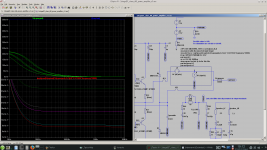
Thanks! Inductance test from V(x) to ground gives bad value 2.8H@1kHz but test signal has about 500mV rms: the safety diodes from rails to output shape the test signal - the results are therefore unusable ...
During capacitance measurement the 1kHz test signal has about 100mV rms so I think the 8nF may be a usable value.
The pcb alone has about 130pF from v(x) to ground and about 80pF from output to each rail. High enough to be inserted into simulation file...
Small signal square wave tests OR why a zobel is always needed
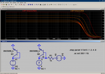
Just measured my second test output stage which is using 8xMJW3281A and 8xMJW1302A instead of 8xTTC5200 and 8xTTA1943.
17nF!
Now I know why I needed stronger compensation to get the OPS using these alternative devices stable...
Just measured my second test output stage which is using 8xMJW3281A and 8xMJW1302A instead of 8xTTC5200 and 8xTTA1943.
17nF!
Now I know why I needed stronger compensation to get the OPS using these alternative devices stable...
Simulation run results:
- Using 8nF parasitic capacitance the gain margin worsens about 10dB
- Using 17nF parasitic capacitance the gain margin worsens about 13dB
I am slightly perplexed. If you are using decent models for the output transistors, said models should be reasonably accurate vis-a-vis parasitic capacitance introduced by the output transistors.
As you have noted, the PCB capacitance by itself is nowhere near the 8 or 17 nF you measure when the PCB is populated, so the majority of the capacitance you measure is coming from the devices.
I doubt therefore that you need to add such a large capacitor to your simulation. The question then arises - why do you need to add the dedicated parasitic capacitance to give simulation results that seem to agree with "real life"? I think this may simply be a coincidence. The reason we add zobels to the output stage is that emitter followers like to "see" a resistive-type load at high frequencies, and without this "parasitic oscillation" can result. Parasitic inductance plays a key role in this oscillation and I think that you should be able to observe oscillation in the simulation by removing your "parasitic" capacitor but adding parasitic inductance. This is particularly challenging as it's difficult to know what the correct values are, and where to place them. Then there is the question of the amount of mutual coupling between those parasitic inductances!
Just as a "sanity check", can you set up a simulation to "measure" the capacitance from output to power ground in your model, without a dedicated parasitic added?
I made those C5200/A1943 models, after measuring the capacitance myself so I know it's correct. So I'd agree with Harry.
I am slightly perplexed. If you are using decent models for the output transistors, said models should be reasonably accurate vis-a-vis parasitic capacitance introduced by the output transistors.
...
Just as a "sanity check", can you set up a simulation to "measure" the capacitance from output to power ground in your model, without a dedicated parasitic added?
Harry: I'm too perplexed. Above I have written "by accident" ...
What I found out is that on adding those 8nF to simulation the small signal square wave figures look exactly like the real world amplifier. The "wiggles" can also be provoked when we undercompensate the simulated amplifier e.g. using 39p or 47p instead of 56p or 68p.
Parasitic inductance will be the next things to be checked (maybe my expensive non-inductive 0.47R are fakes and inductive?).
BTW: the parasitic capacitance from mounted power bjt's to heatsink is about 750pF - also not included in simulation. Currently don't know if this makes any difference between simulation and real life.
Hmm - how to setup a capacitance test in simulation?
Keantoken: I think there is nothing wrong with your bjt models! I like them!
Small signal square wave tests OR why a zobel is always needed
... simulated a ops capacitance measurement from output to powerground with disconnected input stage, disconnected power supply and disconnected output zobel and load.
Stepped "Cparasitic" using 1picoF, 1nF, 8nF, 10nF, 20nF to check if calculation works. Looks like the simulated parasitic capacitance (8,3nF) is nearly exactly the real life measurements.
keantoken's 2SC5200/2SA1943 models are really great stuff!
Can anyone verify if this type of measurement setup and mathematics is correctly? Thanks in advance ...
Attachments
I think this is a bit more simple and direct. Different situations will prefer a voltage or current probe. For this specific test, a voltage probe allows us to measure Cbe vs Vbe regardless of collector current. The current probe only works until Vbe conducts enough to affect the test voltage (which is why the red trace reveals larger capacitance at the last V step).
I switched the plot to cartesian mode and removed the real component of the trace. This way we will see capacitance without it being obscured by resistances such as R1 or Ib.
6.282**-1 to LTSpice means the same as 1/6.282, I just find it more convenient. 6.282**.5 is the same as sqrt(6.282), and so on.
Cbe actually gets enormous as emitter current increases, which is helpful to know when having RF source impedance problems with BJTs.
Attachments
try reducing R49 and R90 to 5r0... simulated a ops capacitance measurement from output to powerground with disconnected input stage, disconnected power supply and disconnected output zobel and load.
Stepped "Cparasitic" using 1picoF, 1nF, 8nF, 10nF, 20nF to check if calculation works. Looks like the simulated parasitic capacitance (8,3nF) is nearly exactly the real life measurements.
keantoken's 2SC5200/2SA1943 models are really great stuff!
Can anyone verify if this type of measurement setup and mathematics is correctly? Thanks in advance ...
This will give an effective 10r+47nF || 10r+47nF across the amplifier output.
i.e. equivalent to about 5r+94nF.
The reduced R90 @ 5r0 will attenuate the interference a little bit more.
On the first schematic from the first page R83=2 ohm and solve the problem. The problem maybe is not from the amplifier and from the CR-LR output filter.
The 10R as part of the output Zobel generally works well for 8ohms capable amplifiers.
I think, but not at all sure, that the 10r should very roughly track the intended output load value.
i.e. for an 8ohms amplifier use ~8r0
for a 4ohms amplifier use ~4r0
for a 2ohms amplifier use ~2r0
There is a big exception:
Some of National's chipamps use a value that is ~ 1/3rd of the nominal amplifier load.
Small signal square wave tests OR why a zobel is always needed
Thank you for your tips. Will try AndrewT changes.
I have added heatsink and pcb capacitance and some inductors to reflect the cable and pcb lengths. In simulation the gain margin worsens about 6db. Now I need to add only 3nF as parasitic capacitance to output with disconnected zobels to get the same results. The used output devices have a relatively high Cbe capacitance. So if we have 16 of those big power bjt's and their specs differ only a few percent to the used simulation models we easily can get 3nF (~ 190pF per device) in sum. Could this be the explanation? Using MJW3281A and MJW1302A need a higher compensation to get the amplifier stable - maybe due to higher Cbe?
Attachments

So if we have 16 of those big power bjt's and their specs differ only a few percent to the used simulation models we easily can get 3nF (~ 190pF per device) in sum.
That's why an amp with low count (read one pair only) of output pairs will always (soundwisely) outperform PA like power amplifiers.

That's why an amp with low count (read one pair only) of output pairs will always (soundwisely) outperform PA like power amplifiers.
Don't think that this is correct. Paralleling output devices reduces noise and distortion. Lower current per device during heavy load keeps them longer linear.
Last edited:
Don't think that this is correct. Paralleling output devices reduces noise and distortion. Lower current per device during heavy load keeps them longer linear.
Technically speaking, first Watt is the most important and reveals all of it.
You need 16 outputs for that?
Nope 😉
Technically speaking, first Watt is the most important and reveals all of it.
You need 16 outputs for that?
Nope 😉
Sorry but I do not want to discuss the component count again like my answer from post 819.
Sorry but I do not want to discuss the component count again like my answer from post 819.
Then why you're constantly asking us members how to improve your amp, eliminate the problems etc.?
My proposal would be, for home use, reduce the parts count, especially the outputs, otherwise you have just another useless high power, high current PA amp.
depends on how you define that first Watt.Technically speaking, first Watt is the most important and reveals all of it.
You need 16 outputs for that?
Nope 😉
Technically speaking, driving a very reactive speaker with music, one will require much more current, than driving a resistor with a constant sinewave.
If you want that first watt to be ONLY in ClassA, then the peak ClassA current will be around an ampere (1Apk).
Technically, that would require an output stage bias current of 1A in a single ended stage, or ~500mA of output bias current in a push pull stage. Borbely, by coincidence or design, has stated that 500mA is the required minimum output bias for a push pull mosFET output stage.
I would prefer load sharing requiring at least two pairs for a push pull output stage to get that "first Watt".
Last edited:
I would prefer load sharing requiring at least two pairs for a push pull output stage to get that "first Watt".
That's exactly what I practice.

- Home
- Amplifiers
- Solid State
- 2stageEF high performance class AB power amp / 200W8R / 400W4R