Hi Toni,
the terms class G and H appear not to be applied consistently to amplifiers like your's. So, may I aks you if it switches or modulates the outer rails? According to the ample power devices count I assum the latter?
Best regards!
the terms class G and H appear not to be applied consistently to amplifiers like your's. So, may I aks you if it switches or modulates the outer rails? According to the ample power devices count I assum the latter?
Best regards!
Dear Kay,
modulation. The output drives the upper mosfets.
The class g/h definition is inconsistent in many documents. NewClassH (NCH) is Dave's and my projects working title.
😎
modulation. The output drives the upper mosfets.
The class g/h definition is inconsistent in many documents. NewClassH (NCH) is Dave's and my projects working title.
😎
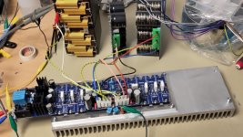
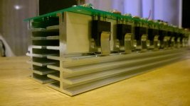
... many days are gone with extensive testing. The prototype has had only one IXYS pair active. With 3 pairs parallel active the situation is difficult. Was a little "odyssey" to get the beast stable at 3-4 R.
A short summary of changes to the above preliminary circuitin some posts ago:
The most changes reflect more or less the values from SA2014. In principle the amplifier is a SA2014 with added NewClassH power stage.
Currently the THD 1k at full power ~ 460W@4R with the 2x55 VAC/800VA transformer is about 0.005%
THD+N 1k 270W@8R is 0.0017%
THD+N 20k 270W@8R is 0.0059%
SNR is > 116dB bw 80kHz vs. full power.
SNR is > 124dB A-w vs. full power.
All measurements taken directly at the load resistors.
The most interesting green fact is running in idle mode the amp keeps cool compared to SA2014.
... and has more power when it is needed.
Have fun, Toni
A short summary of changes to the above preliminary circuitin some posts ago:
- increased LTP degeneration from 82 to 220R
- increased Rbase for TTA/TTC to 4.7R
- increased Rgate to 100R for the IXYS
- removed all 0.1R resistors at the IXYS power stage
- TMC is now 82p/820p/470R
- output zobel 10R/100nF
- emitter resistors of drivers increased to 4.7R
The most changes reflect more or less the values from SA2014. In principle the amplifier is a SA2014 with added NewClassH power stage.
Currently the THD 1k at full power ~ 460W@4R with the 2x55 VAC/800VA transformer is about 0.005%
THD+N 1k 270W@8R is 0.0017%
THD+N 20k 270W@8R is 0.0059%
SNR is > 116dB bw 80kHz vs. full power.
SNR is > 124dB A-w vs. full power.
All measurements taken directly at the load resistors.
The most interesting green fact is running in idle mode the amp keeps cool compared to SA2014.
... and has more power when it is needed.
Have fun, Toni
Attachments
Last edited:

Yes.
IXYS are matched. so no need for the 0.1R
The P-Channel IXYS have a maximum linear use power dissipation of 270W each.
The N-Channel IXYS have higher dissipation in linear mode.
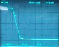
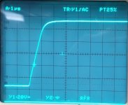
In parallel mode when the currents are very high and the Vds gets low the layout of the board, distance of the MOSFETs gets more and more critically. So I had to slow down the IXYS to get 100% stability running full power square wave at 3.9R
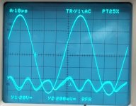
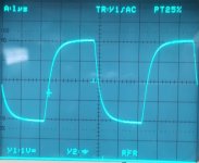
The picture shows the THD+N 20k 270W@8R output wave form and distortion residual measured at the load resistors.
BTW: practically nearly no sticking viewable at overload at 20kHz!
IXYS are matched. so no need for the 0.1R
The P-Channel IXYS have a maximum linear use power dissipation of 270W each.
The N-Channel IXYS have higher dissipation in linear mode.
In parallel mode when the currents are very high and the Vds gets low the layout of the board, distance of the MOSFETs gets more and more critically. So I had to slow down the IXYS to get 100% stability running full power square wave at 3.9R
The picture shows the THD+N 20k 270W@8R output wave form and distortion residual measured at the load resistors.
BTW: practically nearly no sticking viewable at overload at 20kHz!
Attachments
Last edited:
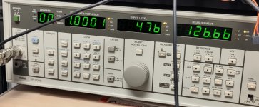
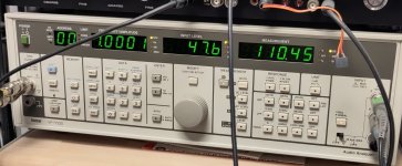
THD+N 1kHz 10W@8R bw 80 is 0.0012%
THD+N 20kHz 10W@8R bw 80 is 0.0036%
The first Watt:
THD+N 1kHz 1W@8R bw 80 is 0.0022%
THD+N 20kHz 1W@8R bw 80 is 0.0022%
(mostly analyzer limit at this low output/input level)
Absolutely acceptable for a green(er) high end amp, what do you mean? 😉
BR, Toni
THD+N 20kHz 10W@8R bw 80 is 0.0036%
The first Watt:
THD+N 1kHz 1W@8R bw 80 is 0.0022%
THD+N 20kHz 1W@8R bw 80 is 0.0022%
(mostly analyzer limit at this low output/input level)
Absolutely acceptable for a green(er) high end amp, what do you mean? 😉
BR, Toni
Last edited:
Doesn't almost any two channel oscilloscope provide the subtraction of both input signals feature?
Best regards!
Best regards!
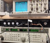
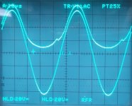
The VP7723D audio analyzer has a separate BNC output on the backside which delivers the distortion residual (after filters e.g. bandwidth 80khz or A-w filter). The first harmonic has been deep notched out.Hi Toni,how do you separate the distortion from the output signal and display it simultaneously on the oscilloscope?
Yes,any dual trace oscilloscope can do it but how to separate distortion waveform from ourput signal?
Now is clean,you have used the audio analyzer for this job.The VP7723D audio analyzer has a separate BNC output on the backside which delivers the distortion residual (after filters e.g. bandwidth 80khz or A-w filter). The first harmonic has been deep notched out.
Thanks Toni.
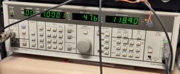
THD+N 1k 277W@8R 0.0009% (power supply limits higher output power)
SNR full bw: 110dB
SNR 80kHz bw: 118dB
SNR A-w: 126dB (my VP7723D limit)
Have fun, Toni
SNR full bw: 110dB
SNR 80kHz bw: 118dB
SNR A-w: 126dB (my VP7723D limit)
- LTP degeneration: back to 82R
- decreased Rgate to 22R for the IXYS
- added 6x Gate/Drain snubbers 2.2n + 22R
Have fun, Toni
Attachments
... now a bit closer to a final version ...
The most important changes are
The most important changes are
- C30 and C31 - increased to 10nF otherwise the slew rate suffers. Now I have a clean >80V slew and tested stable down to 3R load.
- Gate resistors and Gate-Drain snubbers added/changed
- LTP degeneration increased. A hardly measure-able small THD performance lost for stability.
Attachments

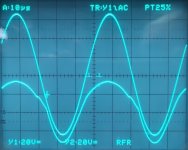
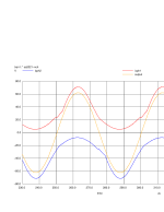
- upper/lower gate voltages @20kHz vs output level
- simulation which corresponds to the real world measurement
Attachments
Last edited:
- Home
- Amplifiers
- Solid State
- 2stageEF high performance class AB power amp / 200W8R / 400W4R